


 Weixin Service

 DouYin
 KuaiShou

Six steps of layer by layer troubleshooting to find out the truth of the short circuit of this sn6505bdbvt
Date:2022-09-01 16:01:00 Views:3395

The reasons for the failure of integrated circuits are complex and diverse. The common reasons are: manufacturing process defects, environmental factorsSMT process, product design defects, EMC design, overvoltage and overcurrent, electrostatic (eSD)Damage, etc.
In this case, the client feedback a batch ofSN6505BDBVTBad output occurs after the driver is mounted on the machine. The defective rate is only0.1% (only 1 failed product). In case of such failure of a mature product, the customer first turned to FAE for front-end troubleshooting, and found no abnormalities in relevant design, peripheral components and welding. Since the reason can not be found from the circuit, the customer sought the help of our core detection, hoping to find out the reason from the components themselves.
exceptFailed sample (NoB1#)The customer also provided oneGood product (NoA1#)For comparative analysis. As for the reason for the failure, you can guess first, and then follow us through the test to verify your idea.
Test process
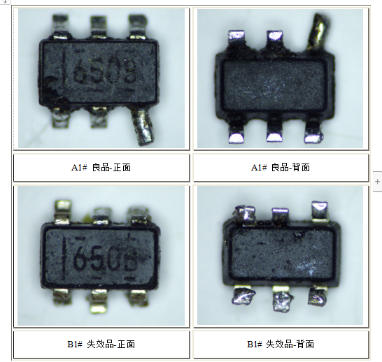
step1: Visual inspection
Purpose:Conduct visual inspection on the received samples to confirm whether the silk screen of the device package is complete, whether there are traces of regrinding and refurbishment, and whether there are obvious damages on the surface of the plastic package, pin integrity and other basic information.
Test results:Check the samples provided, whether they are good products(A1#)Or invalid products(B1#)No traces of secondary coating and re grinding of silk screen were found. In addition, traces of flux residue were found at the tail ends of the pins of the good and failed products, indicating that the two chips were indeed on the machine.
step2: electrical characteristic analysis
Purpose:In order to reproduce the failure of the product, measure the parasitic diode characteristics of the good and bad samples to confirm whether the output terminal is obviously damaged.
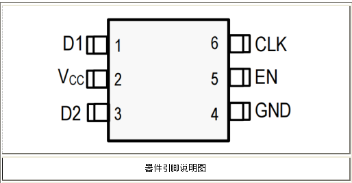
Device pin description diagram:
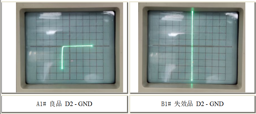
Test conditions:Failed products(B1#)Connect the circuit and connect the oscilloscope and display screenEach grid on the horizontal axis represents the voltage as0.5V,Each grid on the vertical axis represents the current as0.5mA。
result:By comparing with the electrical characteristics of good products, confirm theInvalid productThe diode characteristic curve image between D2 and GND is in short circuit mode, due toD2 is the output terminal. When the D2 drain output terminal of the MOS device is short circuited to the ground, most of the current at the output terminal leaks in the direction of the substrate (GND), causing the level to be directly pulled low.
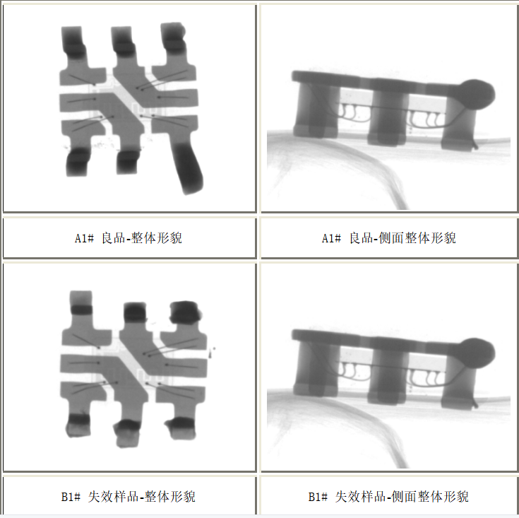
step3:X-RAy inspection
Purpose:After confirming that there is a short circuit, useWhether the internal structure of components is detected by X-rayThere is an exception to verify whether the failure is caused by the packaging problem.
Test results:After comparing the internal images of good products and defective products,No package internal structure, bonding wire andThere are obvious abnormalities in die.In order to find out the cause of failure, destructive tests must be carried out below.
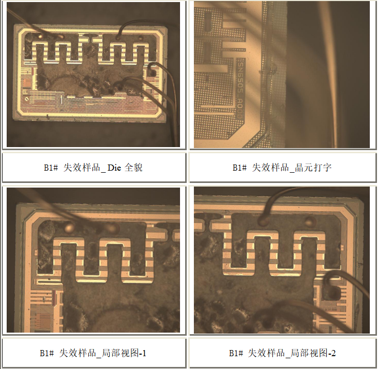
step4: Cover opening inspection
Purpose:Open the lidInspection of defective products(B1#)Whether there are process defects and signs of burning on the die.
Test results:By metallographic examination,stayNo abnormality was found on die.
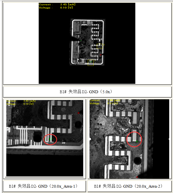
step5: Hot spot analysis(OBIRCH)
objective:Hot spot analysisThe principle is to scan the surface of the chip with a laser, and the energy of the laser beam will be absorbed by the chip and converted into heat. If there is a defect in the chip, the energy at the defect will not be conducted and dispersed, thus causing the temperature at the defect to rise and the resistance value to change.
While scanning,Apply a certain voltage and current to the chipThe voltage and current will change at the defect. The hot spot can be located by scanning the laser to the position where the temperature changes and superimposing the position where the voltage and current change to generate an image.
Hot spot analysisIt can effectively detect the holes of metal wires in the chipThe hole under the through hole and the high resistance area at the bottom of the through hole can also effectively detect short circuit or leakage. stayX-When ray and the cover are not abnormalYes, I'll seeconductCan hot spot analysis open up a situation for us.
Evaluation of test conditions:In order to avoid secondary damageThe power on requirements between d2-gnd are selected as follows: the test voltage is 0.10v, the current is 2.45ma, and the test is conducted at the magnification of 5.0x and 20.0x respectively.
Test results:Hot spot analysis failure sample(B1#), infiveX andAt 20x magnification, two hot spots were observed in die. The next work is to lock their specific positions in the die.
step6: delamination analysis
Purpose:Since the defect points that cause chip failure often occur in the lower layer of the chip, it is necessary to carry out delamination analysis on the hot spot areas found by hot spot analysis to lock the specific location of the sample defect points.
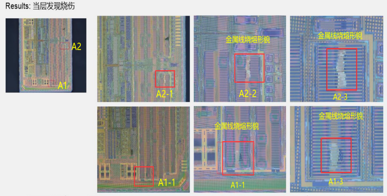
Analysis results:For failed products(B1 #) hot spot analysis abnormal area was analyzed by delamination, and no obvious abnormality was found during delamination of solver, TM and M2,Further de layering toObvious burning marks were found at M1.After the damage point in the chip is identified, we can further analyze and draw the final conclusion of the failure cause.
Delamination analysis steps1—Die_ Solver: no exception found in this layer
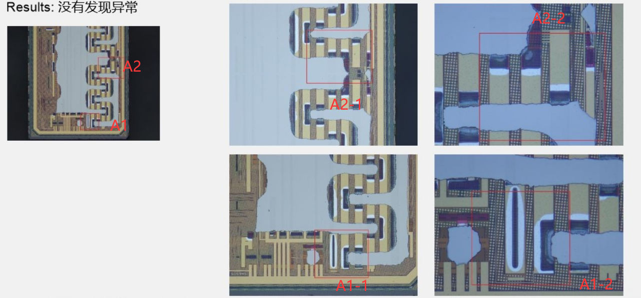
Delamination analysis steps2—Die_ Tm: no abnormality is found in this layer
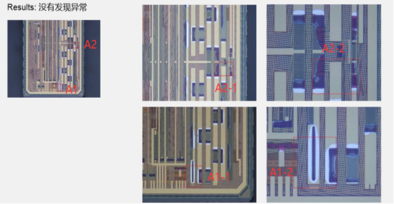
Delamination analysis steps3—Die_ M2: no abnormality is found in this layer
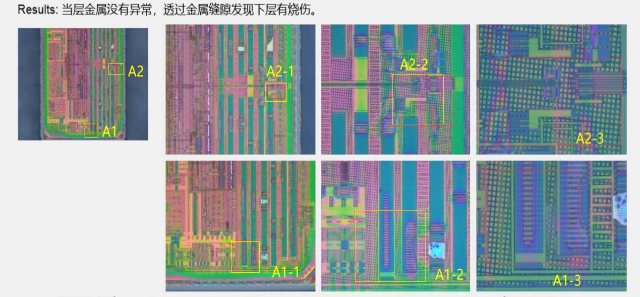
Delamination analysis steps4—Die_ M1: melting point of metal wire found in this layer
Analysis, summary and improvement suggestions
Analysis process:Client feedback modelThe output of sn6505bdbvt driver is poor after it is mounted on the machine, and the defective rate is only 0.1% (1 defective product). Measure the I-V characteristic curve of the failed sample provided by the client, and confirm that there is a short circuit between the output terminal D2 and GND.
In order to explore the final cause of the short circuit, we conductedThrough X-ray and cover opening inspection, no abnormality was found. After further obrich detection and delamination analysis, obvious burn marks were found in M1. Finally, according to the burn morphology of M1, it was confirmed that the failure mechanism was ESD damage.
Conclusion:In summary:The reasons for the poor feedback output of sn6505bdbvt driver client are:ESD damage leads to damage between D2 and GND, which indirectly or directly leads to chip short circuit failure.
Suggestions:Optimize the power grid protection design and pay attention to anti-static measures. Under special conditions, you can refer to theESD prevention and control indicators are tested to further ensure that the whole product has perfect anti-interference capability. In case of material failure, it is recommended that you seek professional IC) help of testing organization,Find out the cause of failure。
Chuangxin online testing center——Your preferenceC testing expert


