What are the common aging screening methods for electronic components?
Date:2022-11-09 15:07:21 Views:2860
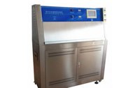
The most widely used screening method is aging, which allows semiconductor devices to overload under high temperature and high voltage conditions, so that defects can appear in a short time. Aging, also known as "sophistication", refers to the continuous application of a certain electrical stress to components at a certain ambient temperature for a long time, which accelerates various physical and chemical reaction processes inside the components through the combined action of electrical thermal stress, and promotes the early exposure of various potential defects hidden inside the components, so as to eliminate early failure products.
_20221109150645_259.jpg)
Common aging screening methods for electronic components
1. Normal temperature static power aging
Normal temperature static power aging is to make devices aged at room temperature. The PN junction of the semiconductor is in a positive biased conduction state, and the thermal stress required for device aging is converted from the power consumed by the device itself. Due to the combined effect of electricity and heat in the aging process of devices, various physical and chemical reaction processes inside the devices are accelerated, which promotes the exposure of potential defects in advance, thus eliminating defective devices. This aging method does not require high-temperature equipment and is easy to operate, so it is widely used. Within the safe range of the device, appropriately increasing the aging power (increasing the junction temperature of the device) can achieve better aging effect and shorten the aging time.
In order to achieve a satisfactory aging effect, the following points should be noted:
① Aging equipment shall be provided with good measures to prevent self-excited oscillation.
② When applying voltage to the device, it should slowly increase from zero, and also slowly decrease when removing voltage, otherwise the transient pulse generated by the sudden change of power supply voltage may damage the device. After aging, it shall be measured in time within the time specified in the standard or specification, otherwise some out of tolerance parameters during aging will return to the original values.
③ In order to ensure the aging of transistors at junction temperature, the thermal resistance of transistors should be accurately measured.
As for integrated circuits, their junction temperature rise is very small due to the large limitation of their operating voltage and current, and it is difficult to reach the temperature required for effective aging without increasing the ambient temperature. Therefore, room temperature static power aging is only used in some integrated circuits (linear circuits and digital circuits).
2. High temperature static power aging
The power on mode and test circuit form of high temperature static power aging are the same as those of normal temperature static power aging. The difference is that the former is conducted at a higher ambient temperature. The junction temperature of integrated circuits can reach a very high temperature because devices are aged at a high ambient temperature. Therefore, generally speaking, the high temperature static power aging effect of integrated circuits is better than that of normal temperature static power aging.
China's military electronic component standards clearly stipulate that integrated circuits should be subject to high temperature static power aging under the specific conditions of aging under the rated power supply voltage, rated load, signal and line specified in the product standards. Aging conditions: 125 ± 3 ℃, 168 h (can be determined as required). Monitor at least every 8 h during aging.
3. High temperature reverse bias aging
During high temperature reverse bias aging, the PN junction of the device is simultaneously subject to high temperature environmental stress and reverse bias piezoelectric stress, and there is no current or only a small current passing through the device, almost no power consumption. This aging method is especially effective for removing early failure devices with surface effect defects, so it is widely used in aging of some reverse applied semiconductor devices.
4. High temperature dynamic aging
High temperature dynamic aging is mainly used for digital devices. This aging method is driven by pulse signal at the input end of the device to be aged, so that the device is constantly in a flipping state. This aging method is very close to the actual use state of the device.
There are two basic test circuits for high temperature dynamic aging: series switch and parallel switch test circuits.
(1) Series switch test circuit is also called "ring counter" circuit. Its characteristic is that the output and input terminals of all tested devices are connected in series to form a ring counting circuit. Since the output of the former stage is the input of the latter stage, that is, the latter stage is the load of the former stage, which requires no external excitation signal and load, the equipment is simple and easy to realize. The disadvantage is that the failure of any device under test will stop the whole ring system and make the test in progress. The test will not return to normal until a new test circuit is replaced or the faulty components are shorted.
(2) The characteristic of parallel switch test circuit is that the tested device is connected in parallel with the excitation power supply, so each tested device can be driven by the external switching voltage independently, and the output end of each tested device can be connected with an analog load, thus overcoming the disadvantage of series switch aging.
The test condition for high temperature dynamic aging is generally 168~240 h aging at rated working temperature and rated working voltage. For example, civil devices usually take a few hours, military high reliability devices can choose 100~168 hours, and aerospace devices can choose 240 hours or even longer.
Aging screening function of components
1. It has a good screening effect for a series of defects that may exist in the process of manufacturing, such as surface contamination, poor lead welding, channel leakage, silicon chip cracks, oxide layer defects and local hot spots.
2. For components without defects, aging can also make their electrical parameters stable.
Aging of components
1. The aging test of resistance elements generally applies power and temperature environment according to the requirements of the specification, and special attention should be paid to whether there is heat dissipation requirement for aging.
2. High temperature voltage aging is generally adopted for capacitor aging test. This method is to apply the rated voltage at the rated working temperature of the capacitor for 96~100 h to eliminate products with breakdown and short circuit caused by defective medium. For example, pinholes, defects and conductive particles in the dielectric of organic film capacitors will lead to capacitor short circuit failure during high-temperature voltage aging; When the seriously defective liquid tantalum electrolytic capacitor is aged at high temperature voltage, the short circuit current flowing through the defect is very large, which makes the product temperature rise suddenly. The electrolyte and solder are rapidly vaporized, so that the pressure is enough to damage the product.
For capacitors without potential defects, high temperature voltage aging can eliminate the internal stress in products and improve the capacity stability of capacitors. High temperature voltage aging can make metallized paper (or plastic foil film) capacitors with defective dielectric produce "self-healing" and restore their performance.
Precautions for high temperature aging
1. The electrical stress of various components should be selected appropriately, which can be equal to or slightly higher than the rated conditions, but it should be noted that new failure mechanisms cannot be introduced when the electrical stress is higher than the rated conditions. For example, when the load of some components exceeds the rated value instantaneously, they will deteriorate or break down immediately. Even if some deteriorated components can work temporarily in the future, their life will also be shortened.
2. After the high temperature aging test, the device can be powered off only when the shell temperature is cooled to below 35 ℃. Under the action of high temperature and no electric field, movable ions can move irregularly, which makes the device's disabled performance return to normal, and may cover up the phenomenon of its once failed.
3. The test after aging test is generally required to be completed within 96 h after the test.
The above is the relevant content of the "commonly used aging screening methods for electronic components" brought about by the core creation test. I hope it can help you, and we will bring more wonderful content later. The company's testing services cover: testing and verification of electronic components, IC authenticity identification, product design material selection, failure analysis, functional testing, factory incoming material inspection, tape weaving and other test items. Welcome to call Chuangxin Testing, we will serve you wholeheartedly.


 Weixin Service

 DouYin
 KuaiShou


