Handling process and precautions of bad BGA welding
Date:2023-03-06 18:26:15 Views:2643
The welding of BGA is an important process of pcba processing. Due to improper PCB design, the problem of bad BGA welding is often encountered. At this time, X-ray fluoroscopy can ensure the reliability of welding connection. So it is very important to diagnose the bad soldering of BGA during reflow soldering of pcba processing. In order to help you understand in depth, this paper will summarize the relevant knowledge of bad BGA welding. If you are interested in the content to be covered in this article, please read on.
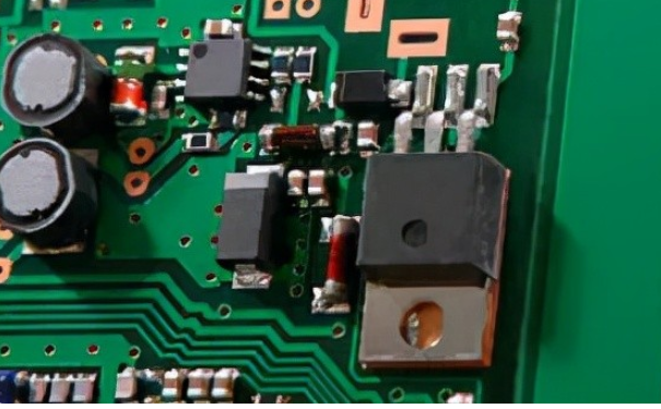
Common BGA welding defects are described as follows:
(1) Blow hole: hole or round pit appears on the surface of tin ball.
Hole blowing diagnosis: during reflow soldering, there is gas overflow in the pores of BGA solder ball.
Hole blowing treatment: use X-Ray to check whether there are pores in the raw material, and adjust the temperature curve.
(2) Cold welding: the surface of the welding point is matt and does not completely dissolve.
Cold welding diagnosis: insufficient heat during welding, and welding spot exposed due to vibration.
Cold welding treatment: adjust the temperature curve to reduce vibration during cooling.
(3) Crystal crack: the surface of the solder joint shows glass crack.
Diagnosis of crystal fracture: when gold is used as the welding pad, crystal fracture occurs when gold and tin/lead are fused.
Crystallization fracture treatment: pre-coat the solder pad of gold with tin and adjust the temperature curve.
(4) Offset: BGA solder joint and PCB solder pad are misaligned.
Deviation diagnosis: incorrect mounting and vibration during conveying.
Deviation diagnosis: strengthen the maintenance of the mounting machine, improve the accuracy of the mounting and reduce the vibration error.
(5) Bridging: solder flows from solder pad to another solder pad to form a bridge or short circuit.
Bridge diagnosis: solder paste and solder ball collapse, poor printing.
Bridging treatment: adjust the temperature curve, reduce the reflux pressure, and improve the printing quality.
(6) Tin splashing: There are tiny tin balls near or between two solder spots on the surface of PCB.
Diagnosis of tin splashing: the quality of solder paste is poor and the temperature rises too fast.
Tin splashing treatment: check the storage time and conditions of solder paste, select appropriate solder paste as required, and adjust the temperature curve.
Welding precautions:
1. Reasonable adjustment of preheating temperature: Before BGA welding, the main board should be fully preheated, which can effectively ensure that the main board does not deform during heating and can provide temperature compensation for later heating.
2. When BGA carries out chip welding, it is necessary to adjust the position reasonably to ensure that the chip is between the upper and lower air outlets, and make sure that the PCB is pulled tightly to both ends with clamps and fixed! The standard is to touch the motherboard with your hand without shaking.
3. Reasonably adjust the welding curve: method: find a flat and invisible main board of PCB, and weld with the curve of the soldering station. When the fourth curve is completed, insert the temperature measuring line of the soldering station between the chip and PCB to obtain the temperature at this time. The ideal value can reach about 217 degrees without lead and 183 degrees with lead. These two temperatures are the theoretical melting points of the above two tin balls! But at this time, the tin ball at the bottom of the chip is not completely melted. From the perspective of maintenance, the ideal temperature is about 235 degrees lead-free and about 200 degrees lead-free. At this time, the chip solder ball will reach the best strength after melting and then cooling.
4. The alignment must be accurate during chip welding.
5. Use an appropriate amount of soldering paste: when welding chips, use a small brush to apply a thin layer on the cleaned pad, and try to apply it evenly. Do not brush too much, otherwise it will affect the welding. During repair welding, a small amount of soldering paste can be dipped with a brush and applied around the chip.
The above is the relevant content of "BGA welding defect treatment process and precautions" brought by this core breaking test. I hope it can help you. We will bring more wonderful content later. The company's testing service covers: electronic component testing and verification, IC authenticity identification, product design material selection, failure analysis, functional testing, factory incoming material inspection, tape weaving and other testing items. Welcome to call Chuangxin Testing, we will serve you wholeheartedly.


 Weixin Service

 DouYin
 KuaiShou


