


 Weixin Service

 DouYin
 KuaiShou

Does the chip fail as soon as it is installed? Look at me using these six steps to identify the true cause of the failure
Date:2023-09-28 17:06:00 Views:6302
introduction
When electronic components are not properly protected or treated in a standardized manner before storage or use, it may cause static damage to the chip, affect its service life, or cause internal circuit breakdown and parameter drift. In severe cases, it may even lead to direct short circuits in some circuits.
This article takes the electrostatic damage (ESD) of chips as an example, analyzes the causes and mechanisms of chip failure through methods such as appearance inspection, I-V curve measurement, X-ray inspection, cover opening inspection, hot spot analysis, and delamination analysis, and proposes improvement suggestions based on actual situations.
1、 Case Background
The terminal customer reported that there was a malfunction during the machine testing, and the PCB board could not operate normally. After cross validation, the locking and positioning of chip A were poor. After conducting impedance measurements on chip A, it was found that the impedance of a certain diode part of the circuit inside chip A was abnormally low. We are conducting testing and analysis to identify the cause of the failure.
2、 Analysis process
▶ 1. Appearance inspection
Firstly, we conducted an appearance inspection on chip A and found that everything on the surface of the chip was normal. We did not find any abnormal phenomena such as damage, cracks, or screen printing that did not match the model.

▶ 2. I-V curve measurement
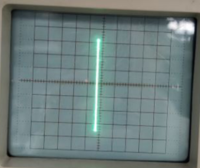
Next, we conducted I-V curve measurement on chip A and found that the I-V curve of the pins between sample PIN4 and PIN5 showed a short circuit phenomenon.
▶ 3. X-ray inspection
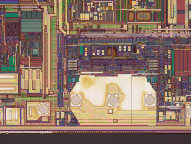
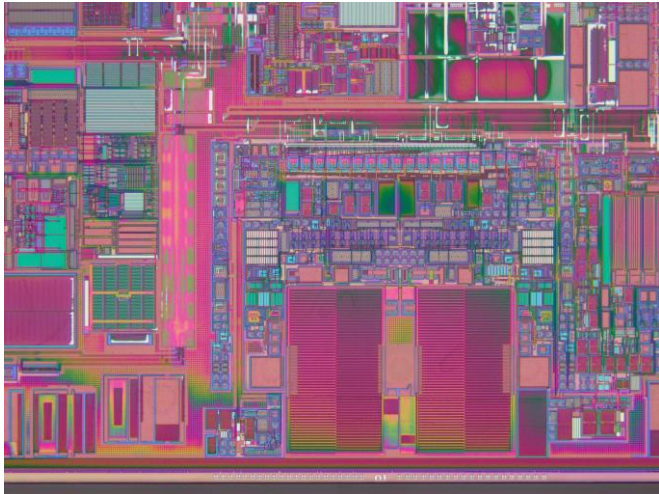
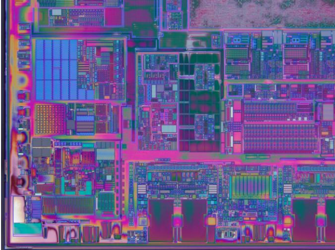
Subsequently, we further conducted X-ray testing on the chip and did not find any abnormal phenomena such as damage to the internal structure and bonding lines of the chip.

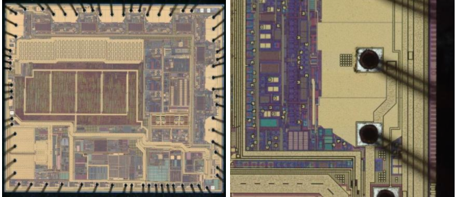
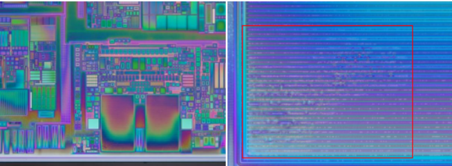
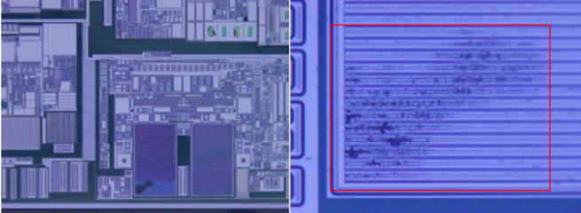
▶ 4. Cover opening inspection
Furthermore, we conducted a cover opening inspection on the chip and did not find any obvious signs of damage.
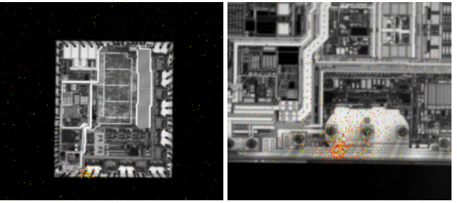
▶ 5. Hot spot analysis
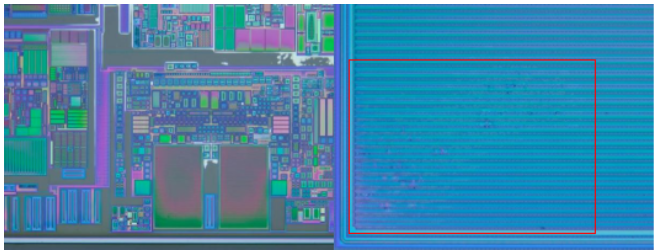
Next, we conducted a hot spot analysis and found that chip A had a short circuit phenomenon based on the I-V curve inspection. In order to confirm the specific location of the short circuit and failure damage points, we used Thermal to locate the hot spot on chip A. From the positioning, it can be seen that the abnormal location is near PIN4-PIN5.
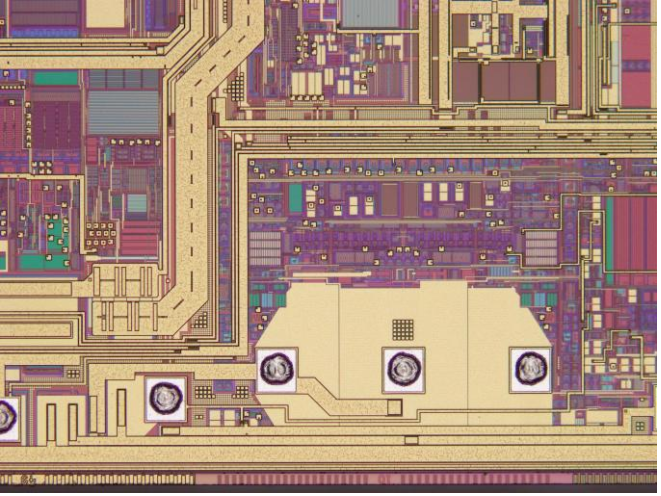
▶ 6. Delamination analysis
Finally, we conducted a delamination analysis based on the location of the hotspots displayed. By layer by layer removal, we found ESD damage in the CT layer until the SUB layer, where the damage was most severe.
RDL layer:
TM layer (M3):
TM layer (M2):
TM layer (M1):
CT layer:
Poly layer:
SUB layer:
3、 Summary analysis
Through visual inspection, it was confirmed that the silk screen of the sample was correct, and no cracks or damages were found.
The V-curve test found a short circuit between PIN4-PIN5 of chip A, which is consistent with the customer's description of an abnormal impedance of an internal diode.
After X-ray inspection and lid opening inspection, no obvious abnormalities were found in the sample.
Through hot spot analysis, it was found that chip A has abnormal hot spots, which are located around the first bonding point of PIN4-PIN5.
Through layer by layer analysis, the hot spots are removed layer by layer, and slight damage is found at the beginning of the CT layer until the SUB layer, where the damage is the most severe.
Overall analysis shows that the chip fails without being installed, with a low failure rate. Additionally, only the diode between PIN4 and PIN5 in chip A is damaged, and no abnormalities were found in the other internal circuits. This may be due to static electricity, which caused the instantaneous high voltage, causing the diode to be instantly broken down and fail.
4、 Conclusion and suggestions
▶ 1. Conclusion
In summary, the direct reason for the failure of chip A is due to ESD damage to internal wafers, which leads to poor chip operation and failure.
▶ 2. Suggestions
Check if storage or operational use is strictly regulated.


