About IC: Introduction to Infrastructure Diodes and Discrete and Integrated Circuits
Date:2024-07-02 10:59:00 Views:3693
A diode is an electronic device made of semiconductor materials, consisting of a PN junction, external leads, and a shell packaging, with the written symbol VD. A diode has two electrodes, the electrode led out from the P region is called the anode (positive electrode), and the electrode led out from the N region is called the cathode (negative electrode); Due to the unidirectional conductivity of the PN junction, the current direction when the diode conducts is from the anode to the cathode through the inside of the tube.
The main principle of a diode is to utilize the unidirectional conductivity of the PN junction. Its essence is that under the action of an applied forward voltage, the holes in the P region and the electrons in the N region are continuously diffusing and moving. The two continuously neutralize the positive and negative ions at the PN junction, thereby narrowing the range of the PN junction and ultimately conducting.
As the most fundamental discrete device, diodes are useful in almost all electronic circuits. The unidirectional conductivity of diodes can play a role in various scenarios such as switching circuits, protection circuits, and voltage stabilizing circuits. With the continuous updating and development of demand, diodes themselves have also developed various forms. The following are more than ten common and commonly used circuit diagram representations of diodes:

The core of a diode is the PN junction, and the construction of this structure needs to be understood from the perspective of wafer fabrication. Semiconductor silicon wafers are divided into N-type wafers and P-type wafers according to the different doping substances. N-type wafers are made by doping silicon crystals with elements (usually phosphorus or arsenic) doped with additional free electrons, which can add additional free electrons to the silicon crystal. P-type wafers are made by doping silicon crystals with elements (usually boron) that can accept electrons. The number of free electrons in silicon crystals decreases, creating "holes" or positively charged spaces.
Entering the diffusion doping process of semiconductor materials, N-type materials and P-type materials are doped in different proportions, and the silicon resistance value can be adjusted. This is the initial material for manufacturing the basic structure of integrated circuits such as diodes and transistors.
Development from Separation to Integration
Looking back at the development history of integrated circuits, as early as the 1950s, vacuum tubes in electronic devices were gradually replaced by transistors, and basic circuit components such as diodes began to be manufactured in the form of transistors. Compared to the original vacuum tubes, transistors have made significant progress in terms of size and lifespan, but the devices are separate and the circuits constructed are still too complex. In the face of this situation, Texas Instruments engineer Jack Kirby arranged diodes, transistors, resistors, capacitors, and other devices on the same substrate and connected them together. This was the original integrated circuit (IC), undoubtedly a groundbreaking invention.
Kirby's integrated circuits are based on germanium (Ge) materials, and it was basically during the same period that Robert Noyce of Xiantong Semiconductor developed integrated circuits based on silicon (Si) materials. Compared to Kirby's circuit which uses flying wires to connect various parts, Noyce directly constructs various devices on the same silicon wafer. In fact, Noyce's invention is closer to today's "chip", with silicon as the material and a manufacturing process similar to transistor planar technology.
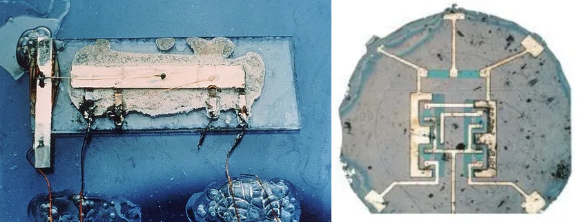
Comparison of integrated circuits between Kirby and Noyes Source: Internet
With the continuous miniaturization of transistor processes, we are able to integrate more basic structures on smaller chip areas. Taking our current product as an example, from the structural diagram of this LM158 operational amplifier, we can see basic structures such as diodes, transistors, resistors, etc. Electronic engineers can understand the specific structure and working principle of the product through this diagram, and then use it reasonably.
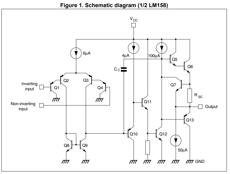
Structure diagram of ST brand LM158 amplifier source: Datasheet of the product
epilogue
Diodes, as important discrete devices, can be found in various circuits. In integrated circuits, it is also an important basic structure. The IC industry has developed to this day, and diodes can be found in various types of integrated circuit structures. Understanding diodes helps us to have a deeper understanding of integrated circuits, starting from the most basic structural hierarchy and mastering the working principles of various devices.
Efficient testing cannot be achieved without familiarity with the components themselves. If customers have needs for failure analysis, appearance inspection, reliability verification, etc., please feel free to call the Chuangxin Online Testing National Hotline at 4008-655-800.


 Weixin Service

 DouYin
 KuaiShou


