


 Weixin Service

 DouYin
 KuaiShou

IC Matters: Application Fields and Failure Factors of IGBT
Date:2024-08-15 11:17:00 Views:5140
Insulated Gate Bipolar Transistor (IGBT) was born around 1980, and its invention was much later than BJT transistor and MOSFET. In this way, this new device naturally combines the advantages of its predecessors. From the equivalent circuit diagram, IGBT is essentially a composite of a MOSFET and a BJT, and also has two characteristics: high input impedance of MOSFET and low conduction voltage drop of BJT.
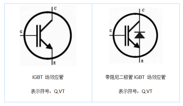
IGBT also has a three terminal structure of gate (G), source (C), and emitter (E). According to the division of P-channel and N-channel in transistors, IGBT also has two forms. However, due to performance differences, the practical application of N-channel is much greater than that of P-channel.
The on resistance of N-channel IGBT is usually lower than that of P-channel IGBT, which means that under the same current and voltage conditions, N-channel IGBT can more effectively reduce power loss and improve energy utilization efficiency. In addition, the switching speed of N-channel IGBT is relatively fast, which can better meet the needs of high-speed switching applications.
The symbol in the above diagram also indicates an N-channel IGBT. Compared to basic devices, IGBT with damping diodes adds one or more damping diodes (usually fast recovery diodes or Schottky diodes) internally to optimize the voltage and current waveforms in the circuit, reducing voltage spikes and current surges during the switching process. For applications that require high-frequency switching, high power output, and good waveform quality, IGBT with damping diode can play a better role.Comparison with MOSFET and other devices
IGBT is a device that combines the advantages of MOSFET and BJT. Can it completely replace the former two, especially MOSFET, in practical applications? The answer is not affirmative. BJTs are currently only used in some extremely cost sensitive applications, while MOSFETs still belong to the mainstream application category due to their own characteristics.
From a practical structural perspective, IGBT is a four layer semiconductor device, manifested as a complex hierarchy of P-type - N-type - P-type - N-type, which enables IGBT to withstand higher voltage and current, and can be used in high-voltage and high current driving scenarios that MOSFETs are not suitable for, such as new energy vehicles, power facilities, etc. MOSFET has a simpler structure and can be driven with low voltage, achieving faster switching frequency. It is suitable for motor driving, LED lighting, and other applications, and can achieve more complex control functions on the premise of simpler circuit design.

Different application ranges of power devices such as IGBT and MOSFET Source: ROHM
From the comparison chart above, the application scope of IGBT and MOSFET has been clearly identified. As for applications that require both high voltage and high frequency, SiC and GaN devices are needed to meet the requirements.
Packaging form: single tube and module
Like various other semiconductors, the manufacturing of IGBT is also divided into steps such as wafer fabrication, etching, cutting into individual pieces, and packaging. But IGBT packaging is different, there are not only single tube packaging, but also module packaging that integrates multiple single tubes together.

Single tube and module packaging IGBT schematic source: Internet
The single tube package mainly consists of an IGBT transistor, a recovery diode, and an optional temperature sensor. Common types include TO247, TO3P, etc. The single tube packaging size is relatively small, and the current capacity is usually below 100A, which is only suitable for low-voltage, low-power power control applications, such as household appliances, small motor control, etc.
Module packaging is much more complex than single tube packaging, which involves integrating multiple IGBT transistors together to form modules with higher power and stronger heat dissipation capabilities. Common forms include 2in1, 4in1, 6in1, etc. In addition to the IGBT transistor itself, the module also contains complex structures such as reverse recovery diodes, temperature sensors, leakage inductance, filtering capacitors, amplifiers, and control circuits. The overall structure of the package is composed of a chip, chip solder layer, upper copper layer, ceramic layer, lower copper layer, base solder layer, substrate, etc., to achieve efficient electrical connection and ensure heat dissipation. Module packaged IGBT is used in high-power fields such as new energy vehicles, high-speed trains, photovoltaics, as well as stability demanding fields such as industrial control and rail transit.
Viewing Failure Types from Module Encapsulation
The failure of IGBT module packaging can be divided into two levels: chip and packaging. Chip level failures include radiation damage, electron migration, electrical overstress, electrostatic discharge (ESD), and other types, which are directly related to the poor working state of IGBT itself. In addition, the failure caused by module structure should also be taken seriously.

IGBT module structure Source: Internet
Package level failures are mainly divided into two types: solder layer failure and bonding wire failure. The manifestation of solder layer failure is the appearance of cracks, voids, or delamination in the solder layer. This type of failure is mainly due to the continuous accumulation of heat generated during the operation of IGBT modules, which generates thermal stress and causes the solder layer to undergo temperature cycling. The manifestation of bonding layer failure is the breakage, peeling or connection failure between the bonding wire and the chip. It is due to the different thermal expansion coefficients between the bonding wire and the module chip. Under the thermal stress of temperature change, the bonding wire will peel off or break. In addition, prolonged high current passing through will also exacerbate the aging and failure of the bonding wire.
The common detection methods for investigating the failure of IGBT modules are X-ray inspection, SAT ultrasonic scanning, scanning electron microscopy (SEM), and metallographic analysis. For various types of failure issues, using specialized methods to investigate the causes and provide improvement suggestions can minimize losses and avoid risks to the greatest extent possible. If you have any questions about IGBT failure, please feel free to call the national hotline of Chuangxin Online Testing at 4008-655-800. We provide professional testing services and offer practical improvement suggestions.


