What are the commonly used methods and techniques for chip failure analysis in laboratories?
Date:2024-08-20 15:00:00 Views:2411
Chip Failure AnalysisIt is an important link in ensuring the quality and reliability of semiconductor products. The commonly used failure analysis methods and techniques in the laboratory include:
1. Optical microscopy examination
· Appearance inspectionObserve the surface defects, solder joint quality, and packaging integrity of the chip using an optical microscope.
· Defect localizationLocate visible defects to assist in subsequent analysis.
2. Scanning electron microscope(SEM)
· Surface morphology analysis: UseSEM observation of the microstructure and defects on the surface of the chip.
· elemental analysis Combined with energy spectrum analysis(EDS), Determine the material composition and element distribution.
3. X-ray imaging
· Internal structure inspection: ThroughX-ray imaging technology inspects the internal structure of chips and identifies potential defects, such as poor soldering and packaging defects.
4. Failure Mode Analysis
· Fault classificationClassify failures, such as electrical failure, mechanical failure, thermal failure, etc., to help determine the cause of failure.
5. Thermal imaging analysis
· Thermal distribution monitoringUse a thermal imaging device to detect the thermal distribution of the chip during operation and identify overheated areas.
6. Electrostatic discharge(ESD testing
· ESD Failure AnalysisEvaluate the performance of the chip under electrostatic discharge conditions and determine its tolerance to static electricity.
7. Electrical testing
· functional testingPerform functional testing on failed chips to check their electrical performance under different conditions.
· Parameter testingMeasure parameters such as current, voltage, and power consumption to help identify failures.
8. chemical analysis
· Material analysisUsing chemical analysis techniques (such asFTIR, XPS) analysis of material composition to determine the presence of material defects or contamination.
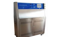
9. Failure Acceleration Test
· Accelerated aging testOperate the chip under extreme conditions (such as high temperature and high humidity) to accelerate the failure process and help analyze the failure mechanism.
10. CT scan(CT)
· 3D imaging: AdoptingCT technology performs three-dimensional imaging on chips, providing more comprehensive internal structural information.
11. Destructive testing
· Cutting and peelingCut or peel off the chip, observe the internal structure and connection situation for in-depth analysis.
12. Current imaging(I-V)
· Current distribution analysisBy using current imaging technology, analyze the current distribution inside the chip and identify potential short circuits or open circuits.
summary
Through the various failure analysis methods and means mentioned above, the laboratory can comprehensively evaluate the causes and mechanisms of chip failure. These analyses not only help improve product design and manufacturing processes, but also enhance the overall quality and reliability of the product.


 Weixin Service

 DouYin
 KuaiShou


