Common methods and steps for surface defect detection of electronic chips in quality inspection
Date:2024-09-23 15:00:00 Views:3674
ElectronicschipSurface defect detection and quality inspection are key steps in ensuring its performance and reliability. Here are some commonly used methods and steps:

1. Visual inspection
· Visual inspectionUse a magnifying glass or microscope to visually inspect the surface of the chip, observing for obvious scratches, cracks, dirt, or other visible defects.
· High definition camera shootingUse a high-definition camera to capture the surface of the chip for post production image analysis.
2. Optical microscopy examination
· Microscopic observationUse an optical microscope to observe the chip in more detail, inspect surface defects, solder joint quality, and other microstructures.
3. X-ray inspection
· X-ray imaging: UseThe X-ray system checks the internal structure and soldering quality of chips, especially suitable for packaging types such as BGA (Ball Grid Array) and CSP (Chip Size Package).
· Defect identificationIdentify internal defects such as voids, short circuits, and poor welding.
4. Scanning electron microscope(SEM)
· High resolution imaging: UseSEM is used for high-resolution imaging to analyze the microstructure and defects on the surface of the chip.
· Spectral analysis(EDX): CombiningEDX conducts elemental composition analysis to check the compliance of materials.
5. Surface contour measurement
· Contouring instrumentUse a surface profilometer to measure surface roughness and shape, and detect possible defects.
6. Electrical testing
· functional testingPerform functional testing on the chip to ensure that it can operate normally under normal working conditions.
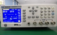
· Parameter testingMeasure key electrical parameters such as current, voltage, and frequency to ensure they are within the specified range.
7. Hot testing
· Thermal cycle testEvaluate the performance and reliability of the chip under extreme temperature conditions through thermal cycling testing.
· Thermal imagingUse a thermal imaging device to detect the thermal distribution of the chip during operation and identify overheated areas.
8. chemical analysis
· Material composition analysisDetect the material composition on the surface of the chip to ensure compliance with specifications and standards.
· Corrosion testingEvaluate the corrosion resistance of chip materials in specific environments.
9. Automated detection
· Machine vision systemUsing machine vision systems for automated detection to improve detection efficiency and accuracy.
· Image processing algorithmApply image processing algorithms to analyze images and automatically identify defects.
conclusion
The surface defect detection and quality inspection of electronic chips require the comprehensive application of multiple detection methods to ensure the performance, reliability, and compliance of the chips. Regular quality inspection and monitoring can effectively reduce defect rates and improve product quality.


 Weixin Service

 DouYin
 KuaiShou


