Wafer fab cleanroom: the micro guardian of semiconductor manufacturing
Date:2024-11-01 09:31:00 Views:5734
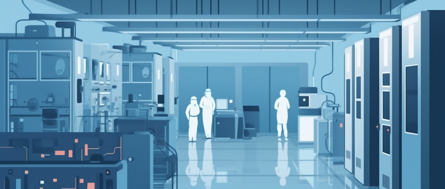
In the precision world of semiconductor components and microfabrication, every tiny dust particle can become a key factor affecting product quality. Therefore, the clean room in the wafer fab has become an important facility to ensure the smooth progress of the semiconductor manufacturing process.
Clean RoomAs the name suggests, it is a closed space designed to isolate dust and other pollutants from entering. In the semiconductor manufacturing process, due to the measurement of space units in micrometers, the adhesion of fine dust particles may have a serious impact on the precise wire layout on the wafer, leading to serious consequences such as electrical short circuits or open circuits. Therefore, the existence of a clean room has become crucial.
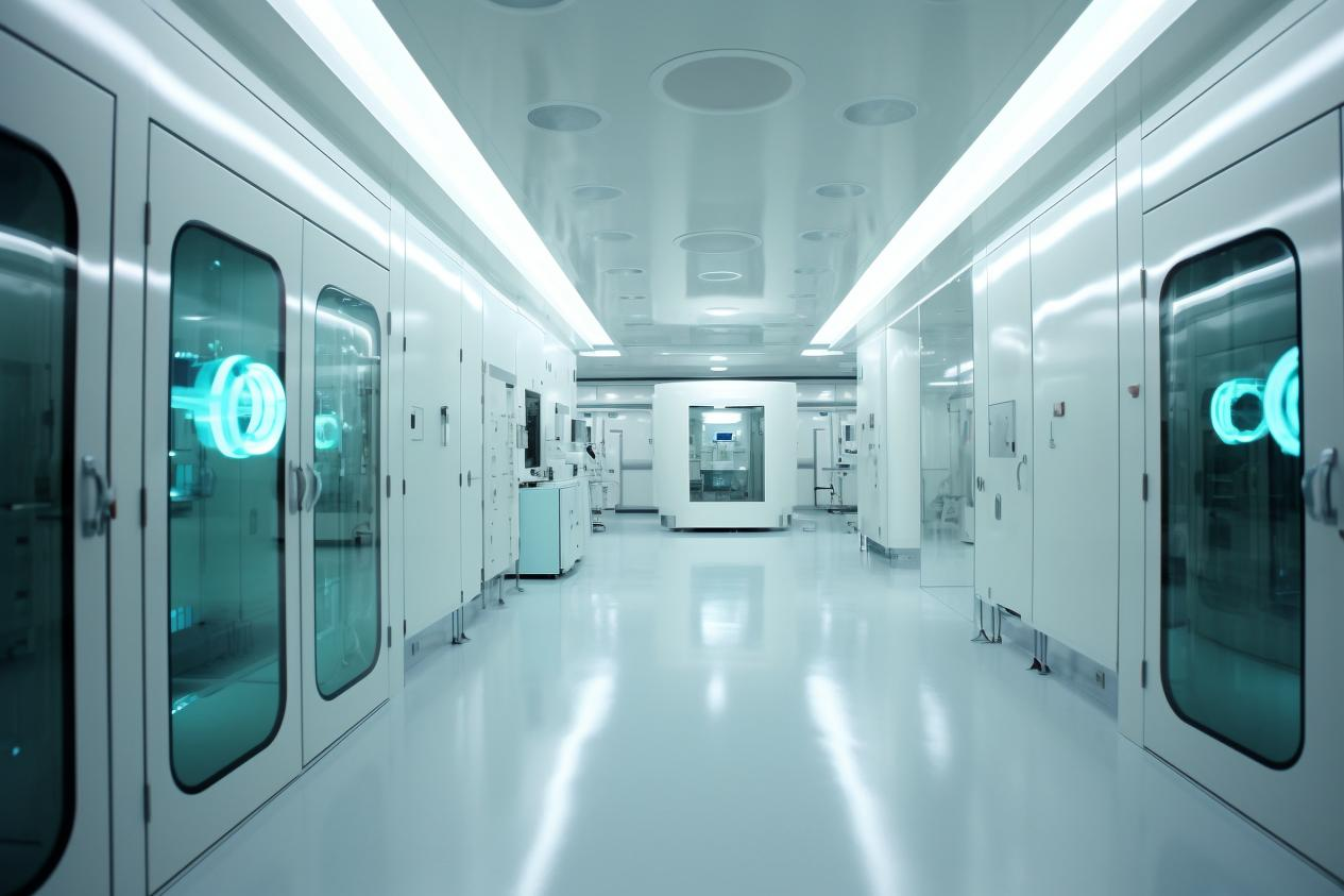
There is a recognized standard for the cleanliness level of a cleanroom. Taking class 10 as an example, this means that on average, there are only 10 particles of dust with a particle size of 0.5 microns or more in a unit cubic foot of space. The smaller the number of cleanliness levels, the higher the cleanliness, but the corresponding cost is also more expensive. This high cleanliness environment is achieved through a series of professional techniques and strict management methods.
Firstly, the cleanroom needs to maintain an environment with a pressure greater than 1 atmosphere to ensure that dust only enters and exits. This is usually achieved by continuously injecting filtered air into the clean room through a large blower. At the same time, in order to maintain constant temperature and humidity, large air conditioning equipment needs to be coordinated with a blower pressurization system.
Secondly, the design of airflow direction in the cleanroom is also crucial. In order to reduce the chance and time of dust swirling and stagnating in the clean room, all airflow directions are mainly from top to bottom. In addition, the interior space design and machine placement of the clean room should also minimize abrupt places.
In terms of building material selection, clean rooms mainly use materials that are not prone to electrostatic adsorption to prevent dust pollution caused by electrostatic adsorption. At the same time, all people and things entering and leaving the clean room must undergo an air bath procedure to remove surface dust.
Hair debris from the human body and clothing is one of the main sources of dust in clean rooms. Therefore, personnel entering and leaving the clean room must wear dust-free clothing and be isolated from the outside world except for the eye area. In factories with sub micron process technology, workers even need to dress as tightly as astronauts. In addition, items such as makeup and pencils that may generate dust are also prohibited from use.
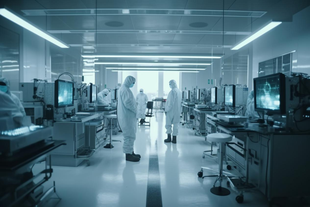
In addition to air, the use of water in clean rooms is also strictly restricted. To prevent contamination of wafers and transistor structures by water particles and heavy metal ions, only deionized water can be used in the clean room. Deionized water is defined as good or bad by its electrical resistivity, which generally requires a resistivity of 17.5 M Ω - cm or higher to be considered qualified. In order to obtain qualified deionized water, multiple ion exchange resins, RO reverse osmosis, and UV ultraviolet sterilization processes need to be used.
In addition, all gas sources used in the clean room, including nitrogen required for drying wafers and machine air pressure, must also meet high purity requirements. The nitrogen used to dry wafers even requires high-purity nitrogen at 99.8% or higher.
In summary, the cleanroom of a wafer fab is an indispensable and important facility in the semiconductor manufacturing process. It provides a high cleanliness environment for semiconductor manufacturing through a series of professional techniques and strict management methods, ensuring product quality and reliability. However, the construction and maintenance costs of clean rooms are also quite expensive, which further highlights their importance in semiconductor manufacturing.
The production of integrated circuits requires strict environmental standards to safeguard them, and in their applications, high-quality protection is also necessary. Shenzhen Chuangxin Online Testing Laboratory (referred to as Chuangxin Testing) is a professional, authoritative, efficient, and innovative component testing institution that has long served the field of component applications. It is a testing institution recognized by the China National Accreditation Service for Conformity Assessment (CNAS) and accredited by the Guangdong Provincial Administration for Market Regulation (CMA).
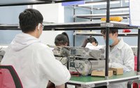
Chuangxin Testing has invested heavily in purchasing various advanced testing equipment and has established three standardized laboratories with an area of over 1800 square meters. The inspection team is composed of hundreds of experienced professional engineers and can provide eight major service projects, including IC authenticity testing, DPA testing, failure analysis, development and functional verification, material analysis, reliability verification, electromagnetic compatibility (EMC), and chemical analysis, providing one-stop solutions for application end customers.
If you have any requirements for component testing,Welcome to call the national hotline of Chuangxin Testing at 4008-655-800 for consultationWe will serve you wholeheartedly.


 Weixin Service

 DouYin
 KuaiShou


