What methods are used for failure analysis? Circuit fault analysis technology
Date:2021-09-09 14:48:00 Views:3030
Failure analysis (FA) is a new developing subject, which has been popularized from military industry to ordinary enterprises in recent years. Generally, according to the failure mode and phenomenon, through analysis and verification, simulate the failure phenomenon, find out the failure cause and mine the failure mechanism. It has strong practical significance in improving product quality, technology development, improvement, product repair, arbitration of failure accidents and so on. The methods are divided into damage analysis, damage analysis, physical analysis, chemical analysis and so on.
Integrated circuit is a kind of micro electronic equipment or components. Using certain technology, the transistor, resistor, capacitor, inductor and other components required by the circuit are connected with the wiring to make a small or several small semiconductor chips or dielectric substrates, which are encapsulated in the tube shell to form a micro structure with necessary circuit functions. The laboratory mainly provides relevant testing and analysis services for integrated circuits.
IC related industries, such as materials, engineering, physics, etc. The development of integrated circuits is inseparable from these related industries. These related industries must be involved in the fault analysis of integrated circuits. The laboratory can also provide micro area observation, element identification, sample morphology processing, fault analysis and other related services.
_20210909144809_253.jpg)
Metallographic microscope / stereomicroscope: provide microscopic image observation, photographing, measurement and other services of samples. The microscopic rate ranges from 10 times to 1000 times. It has the function of light and dark switching, which can be adjusted freely according to the actual situation of the sample and the area of interest.
RIE plasma reactive etching machine: provide chip anisotropic etching function, equipped with CF4 auxiliary gas. On the premise of protecting the metal structure of the sample, it can quickly etch the tungsten, titanium tungsten, silica, rubber and other materials sealed on the chip surface, the protective layer structure, and assist the subsequent experiments of other equipment.
Automatic grinder: provide sample thinning, section grinding, grinding and fixed-point layering services. The automatic grinding equipment has higher efficiency and more accurate force than manual grinding. The factory auxiliary fixture is used to process samples without injection, which is convenient for other experiments.
High speed cutting machine: some chips need profile analysis. At this time, the sample cutting tool can be used to wrap and fix the tested sample with resin, then cut the sample with a high-speed cutting machine with replaceable cutter head, fix the sample to be cut with a fixture, determine the cutting position, and then cut, and spray coolant at the same time. Provide cutting services for PCB or other similar materials and sample resin injection services.
Micro leak detection system (Emmi): low light level microscope (emissionmicroscope), which mainly detects chip power onThe observable fault defects of photons released by the rear internal module fault include junction leakage, contact spike, hotelectrons, latch up, poly silicon whiskers, substratedamage and mechanical damage
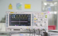
Needle table: provide micro area electrical signal leading out function of chip or other products, support micro level test point signal leading out or application, equipped with hard probe and ox hair needle, which can be used freely according to the actual situation of the sample, and external equipment can be matched freely, such as oscilloscope, power supply, etc. at the same time, the needle head provides sample detail visualization function to assist the chip designer with the help of microscope, Use the needle to contact the chip pin to power up the chip, and observe the power consumption performance of the chip after power on.
X-ray/CT: provide internal perspective images or models of chips or other products. The resolution of X-ray image can reach micron level, which can observe the internal structure, cavity defects and other information of the sample without damaging the sample. CT service is a 3D reconstruction model based on X-ray image, which can scan samples layer by layer more flexibly.
Laser unsealing: high energy laser beam irradiates the chip surface to be opened, and laser high temperature ablation is used to remove the epoxy resin and other substances covered on the chip surface. After the laser is opened, the pins and leads of the chip to be tested are exposed to prepare for subsequent connection or power on test.
IV curve tracker: provide the diode curve drawing function of the chip, and provide the basic positive and negative power on mode. If matched with existing fixtures, the chip can also provide fast batch test, pin custom grouping test diode characteristics.
FIB/SEM/EDX: cooperate with scanning electron microscope (SEM) to selectively remove metal, silicon oxide layer or deposited metal layer with strong current ion beam to complete the processing of micro and nano surface shape. Provide the geometric processing service of sample micro area, bombard the sample with gallium ions to achieve the purpose of micro area processing. The processing range is generally between tens of cubic microns and one cubic micron. The dual beam switching system can provide high-resolution SEM images of the processed area without moving the sample, and provide surface line modification services. Through the combination of FIB and Pt deposition functions, the purpose of line modification can be achieved.
The above is the relevant content of "circuit fault failure analysis" brought by the core detection. Through this paper, I hope it can be helpful to you. If you like this article, you might as well continue to pay attention to our website, and we will bring more wonderful content later. If you have any needs related to the inspection and testing of electronic products, please call Chuangxin testing, and we will serve you wholeheartedly.


 Weixin Service

 DouYin
 KuaiShou


