What aspects need to be tested for incoming PCB inspection? Professional organization testing platform
Date:2021-09-28 15:07:02 Views:3884
Once a company made a statistics to classify the causes of product quality problems. It was found that there are four parts: design, incoming materials, manufacturing process (production) and storage and transportation, accounting for 25%, 50%, 20% and 1 ~ 5% respectively. The problem of incoming materials accounts for 50%, so we come to the conclusion that incoming material inspection is very important. Similarly, in order to ensure the PCB substrates used in the production of SMT production line, these incoming materials must be tested before being put into production to determine whether they meet the production standards. Incoming material inspection is generally carried out by visual inspection in actual production.
PCB incoming inspection includes PCB size and appearance inspection, PCB warpage and distortion inspection, PCB solderability test, PCB solder mask integrity test and PCB internal defect detection.
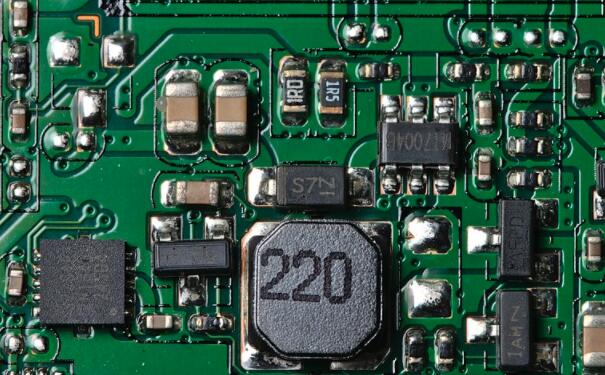
PCB size and appearance inspection
PCB dimension detection mainly includes: diameter detection of machined holes, spacing and tolerance detection, PCB edge dimension detection, etc.
Appearance inspection mainly includes: detecting the alignment of solder resist film and pad; Whether the solder resist film has impurities, peeling, wrinkling and other abnormal conditions; Whether the benchmark mark meets the standard; Whether the width (line width) and spacing of circuit conductors meet the requirements; Whether the multilayer board has peeling, etc. In practical application, special equipment for PCB appearance test is often used to detect it. The typical equipment is mainly composed of computer, automatic workbench, image processing system and so on. This system can detect the inner layer and outer layer of multi-layer board, single / double-sided board and base map film; It can detect broken wire, bonding, scratch, pinhole, line width, line distance, rough edge and large-area defects.
Warpage and distortion detection of PCB
Unreasonable design and improper process treatment may cause PCB warpage and distortion, and its test method is specified in IPC-TM-650 standard. The test principle is: expose the tested PCB to the representative thermal environment of the assembly process and test its thermal stress. Typical thermal stress test methods are rotary immersion test and solder floating test. In this test method, PCB is immersed in molten solder for a certain time, and then taken out for warpage and distortion detection.
The method of manually measuring PCB warpage and distortion is to close the three corners of PCB to the desktop, and then measure the distance from the fourth corner to the desktop. This method can only be used for rough estimation, and the more effective method is the application of ripple image technology.
Solderability test of PCB
PCB solderability test focuses on the test of pad and electroplated through hole. Ipc-s-804 standard specifies the solderability test method of PCB, which includes edge immersion test, rotary immersion test, wave crest immersion test and solder bead test. Edge immersion test is used to test the weldability of surface conductor; Rotary immersion test and wave crest immersion test are used for solderability test of surface conductor and electroplated through hole; Solder bead test is only used for solderability test of electroplated through holes.
PCB solder mask integrity test
On the PCB for SMT, dry film solder resist and optical imaging solder resist are generally used, which have high resolution and no fluidity. Dry film solder resist film is pressed on PCB under the action of pressure and heat. It requires clean PCB surface and effective lamination process. This solder resist film has poor viscosity on the surface of tin lead alloy. Under the impact of thermal stress caused by reflow soldering, it often peels and breaks from the PCB surface. This kind of solder resist film is also brittle. During leveling, microcracks may occur under the influence of heat and mechanical force. In addition, physical and chemical damage may also occur under the action of cleaning agent. In order to expose these potential defects of dry film solder mask, strict thermal stress test shall be carried out on PCB in incoming inspection. The solder floating test is mostly used for this test, the time is about 10 ~ 15s, and the solder temperature is about 260 ~ 288 ℃. When the peeling phenomenon of solder resist film is not observed during the test, the PCB specimen can be immersed in water after the test, and the peeling phenomenon of solder resist film can be observed by using the capillary action of water between solder resist film and PCB surface. PCB specimens can also be immersed in SMA cleaning solvent after the test to observe whether they have physical and chemical interaction with the solvent.
PCB internal defect detection
Microsection technology is generally used to detect the internal defects of PCB. Microsection detection is carried out for PCB after solder floating thermal stress test. The main detection items include the thickness of copper and tin lead alloy coating, the alignment between conductor layers in multilayer board, lamination gap and copper crack, etc.
To sum up, incoming material inspection plays an overwhelming role in the company's product quality, so we should raise the incoming material quality control to a strategic position. The above is the related content of "PCB incoming material detection" brought by the core detection. Through this article, I hope it can be helpful to you. If you like this article, you might as well continue to pay attention to our website, and we will bring more wonderful content later. If you have any needs related to the inspection and testing of electronic products, please call Chuangxin testing, and we will serve you wholeheartedly.


 Weixin Service

 DouYin

 KuaiShou


