


 Weixin Service

 DouYin
 KuaiShou

Main specifications and parameters of MOS field effect tube
Date:2022-03-01 16:38:00 Views:5847
MOS transistor, also known as field effect transistor, is a common power device in the circuit. According to the material structure, it is divided into two types: n-channel MOS tube and p-channel MOS tube. The letter of FET represents the material, D is p-type silicon, and the inversion layer is n-channel; C is the n-type silicon p-channel. For example, 3dj6d is a junction type p-channel field effect transistor, and 3do6c is an insulated gate type n-channel field effect transistor. The following describes the MOS FET parameter comparison table and main specifications.
FET viewing parameters
1. K3878 is a field effect transistor. There are two naming methods for its model. The first naming method is the same as that of bipolar triode. The third letter J represents Junction FET and O represents insulated gate FET.
2. The second letter represents the material, D is p-type silicon, and the inversion layer is n-channel; C is the n-type silicon p-channel. For example, 3dj6d is a junction type p-channel field effect transistor, and 3do6c is an insulated gate type n-channel field effect transistor.
3. The second naming method is CS ××#, CS stands for field effect transistor, ×× Numbers represent the serial number of the model, # and letters represent different specifications in the same model. For example, cs14a, cs45g, etc.
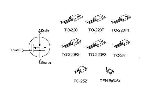
Packaging form:
After the MOSFET chip is made, it needs to add a shell to the MOSFET chip, that is, MOS tube package. The shell of MOSFET chip has the functions of support, protection and cooling. At the same time, it also provides electrical connection and isolation for the chip, so that MOSFET devices and other components form a complete circuit. According to the way of installation on PCB, MOS tube packaging mainly includes two categories: through hole and surface mount. Plug in is that the pin of MOSFET is welded on the PCB through the mounting hole of PCB. Surface mount is that the pins of MOSFET and heat dissipation flange are welded on the pad on the surface of PCB.
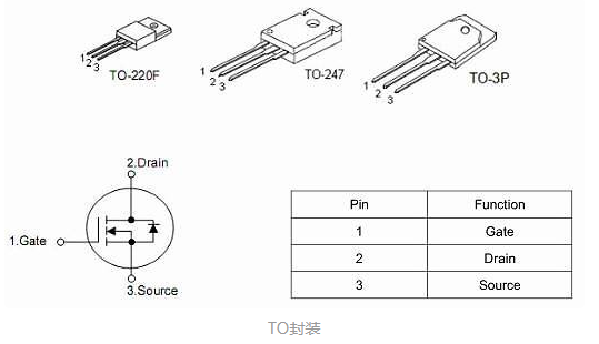
To package specification
1. To (transistor out line), in Chinese, is an early packaging specification. For example, TO-92, to-92l, TO-220, TO-252, etc. are plug-in packaging designs.
2. In recent years, the increasing demand of surface mount market also makes to packaging progress to surface mount packaging. To252 and to263 are surface mount packages. TO-252 is also called D-PAK, and to-263 is also called D2Pak.
FHP, FHF and FHA are TO-220 to-220f to-3pn corresponding to these three. Among them, FHP is TO-220, the packaging form is iron head, FHF is to-220f, the packaging form is plastic packaging, and FHA is to-3pn.
Main parameters of FET
1. On voltage UT (MOSFET)
Generally, the gate source voltage corresponding to the newly formed conductive channel and the emergence of drain current ID is called the on voltage, which is represented by UGS (th) or ut.
The on voltage UT is a parameter of MOS enhanced transistor. When the gate source voltage UGS is less than the absolute value of the on voltage, the FET cannot be turned on.
2. Pinch off voltage up (JFET)
When the UDS is a fixed value (such as 10V) and the ID is equal to a small current (such as 50mA), the voltage applied between the grid and the source is the pinch off voltage. When UGS = up, the drain current is zero.
3. Saturated drain current IDSS (JFET)
The saturated drain current IDSS is the drain current when the FET is pre clamped off under the condition of UGS = 0. The maximum current that IDSS FET can output.
4. DC input resistance RGS
The DC input resistance RGS is the DC resistance between the grid and the source when the drain source is short circuited and the grid source is applied with voltage.
Junction FET: RGS "107 Ω, MOS transistor: RGS" 109 ~ 1015 Ω.
5. Transconductance GM
The ratio of the micro variable of drain current to the micro variable of gate source voltage, i.e. GM = △ ID / △ UGS. It is a parameter to measure the ability of FET grid source voltage to control drain current. GM is equivalent to HFE of triode.
6. Maximum drain power consumption
Maximum drain power consumption PD = udsid, equivalent to PCM of triode.


