


 Weixin Service

 DouYin
 KuaiShou

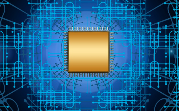
What are the analysis methods of semiconductor chip failure analysis?
Date:2022-03-04 13:57:14 Views:3155
Semiconductors are mainly composed of four components: integrated circuits, optoelectronic devices, discrete devices and sensors. Since integrated circuits account for more than 80% of devices, semiconductors and integrated circuits are usually equivalent. From computers and smart phones to automotive electronics and artificial intelligence, we can see them everywhere in our production and life. The key to their development is the semiconductor chip that drives the internal transceiver. With the expansion of application scenarios and market, the demand for semiconductor chips will undoubtedly increase, and there are higher requirements for their quality.
There are many reasons for failure, such as fracture, deformation, surface wear and so on. Correct failure analysis is the basic link to solve the failure of parts and improve the bearing capacity. Failure law and mechanism are the basis of material strength research. Study the failure causes from the perspective of materials, and then find an effective way to prevent failure.
For chip manufacturers, it is far from enough to simply know whether the chip meets the standard, so as to eliminate bad products and ensure the quality of output products. We also need to "know why", ensure the yield, trace the source, and create higher benefits for the enterprise while saving costs. Therefore, around this theme, a series of tests will be carried out, which we call semiconductor failure analysis. Its significance is to determine the failure mode and failure mechanism of semiconductor chip, so as to pursue responsibility and put forward corrective measures to prevent the recurrence of problems.
Common analysis methods:
1. X-ray nondestructive testing can be used for testing
*Various defects in IC packaging, such as layer peeling, burst, cavity and integrity of wiring
*Possible defects in PCB manufacturing process, such as poor alignment or bridging
*Defects of open circuit, short circuit or abnormal connection
*Solder ball integrity in packaging
2. Sat ultrasonic flaw detector / scanning ultrasonic microscope
It can carry out non-destructive detection on the internal structure of IC package, and effectively detect various damages caused by water, gas or heat, such as:
Wafer surface delamination
Cracks in solder balls, wafers or filler
Pores inside the packaging material
Various holes, such as holes at the wafer joint surface, tin ball, glue filling, etc
3. SEM scanning electron microscope / EDX energy dispersive X-ray apparatus
It can be used for material structure analysis / defect observation, element composition, conventional micro area analysis and accurate measurement of component size
4. Common leakage current path analysis means: Emmi low light microscope Emmi low light microscope is used to detect abnormalities caused by ESD, latch up, I / O leakage, junction defect, hot electrons, oxide current leakage, etc.
5. Probe station / probe test probe test can be used to directly observe the internal signal of IC
6. ESD / latch up ESD / latch up utility test
7. FIB cut point analysis
8. Package removal
Advanced capping equipment and rich operation experience can safely and quickly remove various types of chip packaging, and provide professional chip capping and grain removal services.
The above is the related content of "semiconductor chip failure analysis" brought by the core creation test. I hope it can be helpful to you. We will bring more wonderful content in the later stage. The company's testing services cover: electronic component testing and verification, IC authenticity identification, product design and material selection, failure analysis, function testing, factory incoming material inspection, tape braiding and other testing items. Welcome to call Chuangxin testing. We will serve you wholeheartedly.


