Common screening methods and selection principles of electronic components
Date:2022-11-25 16:16:57 Views:2886
Electronic components shall be selected according to the electrical performance, reliability and manufacturability requirements of the product, and the types, dimensions and packaging forms of components shall be selected. Conventional components shall be selected as far as possible.Ensure that the electronic components meet the requirements of design documents and process documents, and the components and printed circuit boards selected for assembly shall be compatible with the characteristics of the process materials used in the assembly process.
Generally, the components shall be in tubes, tapes or boxes.The selected electronic components shall be consistent with the design standards and suitable for the process and equipment standards.The solderability, heat resistance and cleaning resistance of components must meet the requirements of assembly and welding characteristics.
The solderability of purchased components shall be the responsibility of the supplier, which shall meet the specified requirements. Before the acceptance of components, the manufacturer shall ensure that the components have been solderability tested according to the sampling plan and meet the applicable solderability specifications.When ordering components, it is required that the coating thickness of tin coated lead alloy lead wire shall not be less than 7.5 um and the tin content in the coating shall be between 60% and 63%.After the components are unpacked, they shall be stored at a temperature of 25 ℃± 2 ℃ and a relative humidity of 30%~70%. They shall be welded within 48 hours of storage. The solderability of the components' leads and welding ends shall still meet the technical requirements for solderability.
Designers need to know the materials and coating compositions of the component leads or welding ends selected for the product, and provide relevant data to the technologists.Complete variety.Quality and dimensional accuracy of components.Pay attention to the assembly process requirements of SMC/SMD, the mounting pressure, impact force and welding requirements that components can withstand, especially the technical requirements of BGA, CSP and lead-free welding.Determine the type and quantity of components, minimum spacing and minimum size of components.The identification of lead-free components shall be marked in the list of assembly components to clearly distinguish lead/lead-free components for identification and processing separately in terms of process methods.
The designer shall consider the assembly, testability (including visual inspection) and maintainability of components; In principle, SMD/SMC that does not meet the heat resistance requirements of wave soldering and reflow soldering shall not be used; If necessary, SMD/SMC with welding temperature below 250 ℃ shall be described in the circuit design document; QFP with pin spacing less than 0.5mm shall be carefully considered.The designer shall consider whether the data related to manufacturing are complete and available (such as the complete and detailed outline dimensions of components; pin materials, process temperature limits, etc.).
_20221125161614_259.jpg)
Common methods for secondary screening of components
Screening tests can be divided into conventional screening (such as airtight screening) and special environmental screening (such as radiation resistance, salt spray, etc.).
Common screening methods mainly include the following:
1. Check and screen
Microscopic examination, infrared screening and X-ray screening can be adopted for inspection and screening. Infrared screening can remove the components with serious thermal defects in the body or surface. X-ray screening is mainly used to check whether there are foreign objects, defects in the chip mounting, bonding or packaging process and chip cracks in the shell.
2. Sealing screening (such as bubble method, helium mass spectrometer method, radioactive gas, tracer leak detection method) is used to remove defects (such as cracks, tiny leaks, air holes and poor packaging alignment) in the tube shell and sealing process.
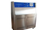
3. Environmental stress screening (such as vibration acceleration, impact acceleration, centrifugal acceleration, temperature cycle and thermal shock);
4. Life screening (high temperature storage, low temperature storage, aging screening, precision screening, linear discrimination);
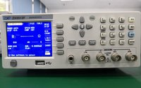
5. Electrical test screening (supplementary means for transistors).
In practice, the combination of physical screening (non-destructive) and sophisticated screening (destructive) is often used. Experienced screening has good effect but high cost, while physical screening has low cost but poor effect.
In the development and production of military equipment, the secondary screening (supplementary screening) of components is mainly applicable to the following situations:
The component manufacturer did not conduct a screening.
The user of components cannot obtain the information of primary screening, and does not understand the items and stresses of primary screening. This is the case for most imported components.
The items or stresses screened by the component manufacturer at one time cannot meet the quality and reliability requirements of the user for components. The screening requirements of component users are generally determined by the overall model unit.
For some special screening items, there are no specific provisions in the product specifications of components, and the manufacturers of components do not have screening conditions.
Components that need to be verified if the component manufacturer has conducted a screening or has doubts about the effectiveness of the primary screening according to the requirements of the contract and specifications.


 Weixin Service

 DouYin
 KuaiShou


