


 Weixin Service

 DouYin
 KuaiShou

Common methods to improve reliability in integrated circuit design
Date:2021-07-23 16:52:00 Views:4935
The basic principle of improving reliability in integrated circuit design is to combine the requirements for devices with specific process conditions. Therefore, familiarity with process characteristics is the basis of good design. In circuit design, the following measures can be taken to improve the reliability of integrated circuits:
(1) Clarify the circuit technical indicators and use environment.
(2) Reduce area and complexity. On the basis of meeting the functional requirements, simplify the circuit to minimize the total area and complexity and reduce the number of contacts (such as reducing the number of isolation islands of bipolar integrated circuits). The reduction of area can reduce defects and improve reliability.
(3) A certain tolerance is given to circuit devices, that is, design according to the worst case, which is also called tolerance design.
(4) Under the same parameter index, the power consumption of the circuit shall be reduced as far as possible (for example, the working current shall be selected appropriately), so as to reduce the junction temperature and improve the reliability; When the maximum current Imax ≤ 2 × At 10 ^ 5A / cm2, it is also conducive to prevent electromigration.
(5) When necessary, consider the redundancy design of components, that is, add parallel or series components to ensure reliability, which is often considered in the design of components or complete machine.
(6) Add protection circuits in some circuits, such as overvoltage protection and overcurrent protection in the integrated voltage regulator, overcurrent protection circuit in the output stage of the integrated operational amplifier, temperature compensation circuit in the circuit with high temperature stability, input protection circuit at the input end, etc. The following focuses on the input protection network against electrostatic breakdown (ESD) at the input end of CMOS integrated circuits.
1。 Diode and resistance double-layer ESD protection structure
Using diode and resistance double-layer protection structure to clamp ESD and filter discharge charge is a common protection circuit technology. This protection technology is used in early NMOS circuits, and this ESD structure is also used in some small-scale CMOS circuits at present. A simple diode can be used as a clamping unit to suppress ESD when it is positively biased. Its on resistance (RON) is relatively low, about 10 Ω, and the trigger voltage is also relatively low. On the other hand, when the diode is reverse biased, its characteristics as a clamping unit are poor. At this time, its Ron is very high, about 100 Ω, resulting in great energy consumption. This ESD structure design and process conditions are relatively simple, and it is a common form of ESD protection circuit. For micron CMOS integrated circuits with antistatic requirements, the protection circuit shown in Fig. 1 can be used. D2, D4, D6 and D8 are distribution diodes of P + diffusion resistance. D1, D3, D5, D7 and D9 are diodes formed by p-n + junctions.
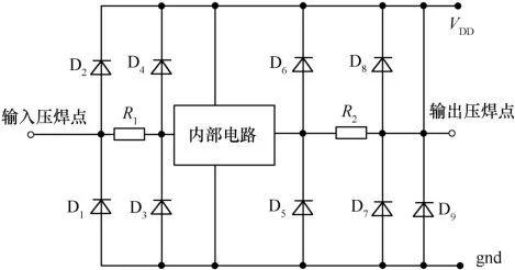
Figure 1 Basic diode and resistor double-layer ESD protection structure
Using diode clamping and RC low-pass filtering, the ESD charge pulse at the port can pass through the protection network bypass to avoid entering the circuit, and other interferences at the port can also be filtered out.
2. Gg-nmosesd protection structure
In CMOS integrated circuit technology, gg-nmos (gate, source and lining grounded NMOS) ESD protection structure is the most widely used ESD protection measure at present, which is mainly used for ESD protection of micron and submicron CMOS integrated circuits. Figure 2 shows the typical gg-nmos ESD protection structure. Gg-nmos ESD protection structure uses snapback characteristics to clamp transient high voltage and shunt. It has the characteristics of low clamping voltage and low opening resistance, while diode ESD protection structure has large opening resistance. When a positive pulse (ESD) is applied to the drain junction (n + / P), the junction is reversed and the device enters a high impedance state until the breakdown voltage is reached. Due to the high field state, electron and hole pairs are generated in the depletion region, the electrons are collected by the drain contact electrode, and the holes are collected by the substrate contact electrode. Relative to the grounded source junction, the local potential of the substrate increases. When the local potential increases enough to bias the source substrate junction, electrons are injected into the drain region from the source region.
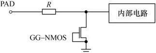
Figure 2 gg-nmosesd protection structure
3。 Parasitic PNP and npnesd protection structure
The fully parasitic bipolar PNP and NPN Transistor ESD protection network can effectively avoid the diffusion of a few carriers in the clamping current generated by PN junction clamping or MOS tube clamping structure to the internal circuit area. Its structure is shown in Fig. 3.
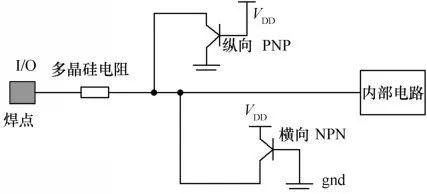
Figure 3 parasitic PNP and NPN ESD protection structure
In this ESD protection circuit, polysilicon resistor absorbs most of ESD energy. This protection circuit is actually formed by P + and N + diffusion regions, and its clamping mode is PN junction clamping. The diode formed by P + diffusion region and n-well form a parasitic vertical PNP transistor. The well collecting ring surrounds the N region and the substrate, collects most of the minority carriers injected into the substrate by ESD discharge, and acts as the collector of the transverse NPN transistor. The protection circuit can clamp the wiring to the internal circuit between Vdd and VSS (ground) potential during electrostatic discharge. Fig. 4 is the layout of parasitic PNP and NPN ESD protection structure based on n-well CMOS process.
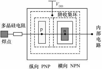
Fig. 4 layout of parasitic PNP and NPN ESD protection structure based on n-well CMOS process
4. Scresd protection structure
The ESD protection structure with parasitic transverse pnpn structure (SCR) is the most effective and widely used ESD protection structure at present. It has the characteristics of high current suction / output, low on impedance and large heat dissipation volume. However, SCR devices need a high trigger voltage. At the same time, in order to perform the protection function, the trigger voltage must be less than the damage voltage of the input buffer or output driver. According to the experiment, the diffusion of LDD and silicon is 1 μ M CMOS process, and the distance between anode and cathode is 6 μ The trigger voltage of M parasitic transverse SCR device is 50V, so a separate parasitic transverse SCR cannot be used as the only ESD protector. In order to provide a wider range of ESD protection, secondary protection elements such as resistors and diodes were mostly used in the early SCR four-layer structure protection circuits. In order to reduce the secondary protection elements, some researchers use two methods to reduce the parasitic transverse SCR trigger voltage. One way is to integrate a short channel NMOS transistor with low breakdown voltage in the transverse SCR to form a "lvtscr" structure. The trigger voltage of this structure is generally 10 ~ 15V, but it is difficult to combine this NMOS transistor with the transverse SCR. Another solution is to add an "NLCs" mask to complete the field injection deep in the transverse SCR in order to obtain a lower trigger voltage. The minimum trigger voltage obtained by this method is 9V. The disadvantage of this method is to increase the mask and process steps, which is not widely used.
At present, the ESD protection circuit with double parasitic transverse SCR structure is widely used, as shown in Figure 5. In this ESD protection circuit, one parasitic transverse SCR structure is arranged to discharge positive ESD pulses, and the other is arranged to discharge negative ESD pulses. Both SCRs have a lower trigger voltage. In this ESD protection circuit, there is no breakdown of PN junction or device. This avoids performance degradation caused by device or junction breakdown after several ESD transients. The protection circuit has small layout size, low input capacitance and low on resistance. It ideally meets the design requirements of ESD protection circuit on CMOS circuit chip. Fig. 6 is a layout of one of the scresd protection circuits.
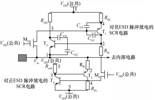
Fig. 5 double parasitic transverse scresd protection structure
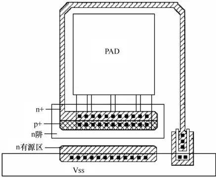
Fig. 6 scresd protection structure layout


