


 Weixin Service

 DouYin
 KuaiShou

What measures will be taken to improve the reliability of integrated circuit layout design?
Date:2021-07-23 17:09:29 Views:5496
Integrated circuit layout design refers to mapping the circuit design circuit diagram or circuit description language to the physical description level, so that the designed circuit can be mapped to the wafer for production. Layout is a graph containing relevant physical information such as device type, device size, relative position between devices and connection relationship between devices of integrated circuit. These graphs are composed of graphs located on different drawing layers. Integrated circuit design method involves a wide range and complex content, in which layout design is the basic technology of integrated circuit physical implementation.
According to the temperature range used (Military - 55 ~ 125 ℃, civil - 25 ~ 85 ℃) and other reliability requirements, electrical and thermal properties need to be considered in layout design. The structure and size of components are determined according to the requirements of electrical parameters and process level, and then the parasitic effect and heat dissipation are considered, so as to finally determine the layout and wiring of the whole circuit. The following are the general measures to improve the reliability of integrated circuit layout design.
_20210723170820_801.jpg)
1. About metallization layer wiring
A large number of failure analysis shows that the failure caused by the short circuit between the metallized layer (generally Al layer) through the pinhole and the substrate and the open circuit of Al film wiring can not be ignored, so preventive measures must be taken in the design of wiring. For example, try to reduce the coverage area of Al strip, use the shortest al strip, and try to distribute al strip on the thick oxide layer (the parasitic capacitance of the thick oxide layer is also small) to reduce the possibility of pinhole short circuit.
The main way to prevent open circuit of Al strip is to pass through oxide steps as little as possible. If steps must be crossed, reduce the height and slope of steps.
In order to prevent electromigration failure caused by excessive current density of Al strip, the current density j passing through al strip is required to be less than 2 × 10 ^ 5A / cm2, Al strip must have a certain width and thickness.
For multi-layer metal wiring, the number of wiring layers and channels between layers in layout design shall be as few as possible.
2. Heat distribution in layout design
It is speculated that the failure rate will double when the chip temperature increases by 25 ℃, so the chip temperature should be reduced as much as possible to reduce the failure rate. In order to prevent the junction temperature from being too high, the area of the tube with large power should be designed large enough, and the effective side length of the emission area is still determined by the maximum current. The layout and distribution of heating elements on the whole chip shall be uniform, so as not to concentrate the heat too much in one corner. In the layout of elements, elements easily affected by temperature shall also be arranged away from heating elements. In the circuit that must be matched, the corresponding elements can be configured side by side or axisymmetrically to avoid lithography dislocation and uneven diffusion. Pay attention to the position of the power cord and ground wire. These wires should not be too long.
3. Other measures
(1) The selection of component size shall be appropriate. Factors such as power density, parasitic effect, plate making lithography error, transverse diffusion and diffusion tolerance shall be considered. Al strip shall cover ohmic contact hole and leave a certain margin.
(2) Ensure the requirements of circuit parameters: the long neck area of multi emitter transistor should not be too long, because too long will lead to the decrease of FT; Avoid making diffusion "ground" channel on the output line; The ohmic contact hole connected to the power supply on the resistance island of the epitaxial layer shall be expanded by N +.
In addition, for CMOS integrated circuits, in order to improve their anti latch ability, the following measures can be taken in layout design: ① reasonably arrange power contact holes to reduce transverse current density and transverse resistance; ② Adopt the annular VDD power line (p-well) connected to the substrate, and connect the back of the substrate to VDD as far as possible; ③ Increase the contact holes of power Vdd and VSS (GND) and increase the contact area; ④ For each hole connected to VDD, corresponding VSS (GND) contact holes shall be equipped in the adjacent wells to increase the parallel current path; ⑤ Try to make the long sides of the contact holes of Vdd and VSS parallel to each other; ⑥ The hole connected to VDD shall be arranged as far away from the well as possible; ⑦ The holes connected to VSS should be arranged on all sides of the p-well as far as possible.
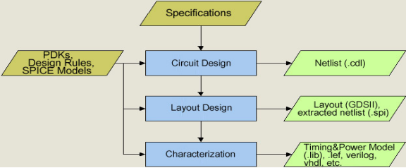
The function of IC layout design rules is to ensure the circuit performance, easy to realize in the process, and can achieve high yield.The quality of layout design will directly affect the power consumption, performance and area of integrated circuits.In the design of system on chip (SOC), interface unit (input / output, I / O), standard cell, analog mixed signal (AMS) module, memory (such as ROM, RAM) and a variety of IP modules are integrated. The physical implementation of all these modules is inseparable from the basic layout design.In engineering practice, after defining system chip specifications, people often simplify the layout design process of standard logic units in the most common digital integrated circuits into three steps: circuit design, layout design and characterization. See the simplified layout design flow chart in Figure 1. In practice, layout design types are divided into: 1) standard layout design, 2) semi custom layout design, and 3) full custom layout design.
Conclusion: whether it is standard cell layout design, semi custom layout design or full custom layout design, the basic design methods have been carried forward and inherited, and the requirements of high performance, low power consumption and low cost have been raised higher, which has set a new standard and starting point for high-quality and high reliability layout design in the future.


