


 Weixin Service

 DouYin
 KuaiShou

Electronic component testing center: failure mode and effect analysis
Date:2021-08-23 13:55:14 Views:4672
As the basic force of electronic information industry, electronic component industry is the focus of development and innovation in the new era. The development process of China's electronic components is from shallow to deep, from less to more, until it accumulates to a certain extent. According to statistics, at present, the total output value of China's electronic components industry accounts for about 20% of the electronic information industry. The electronic components industry has also become the basic content to guide the sustainable development of China's electronic information industry. Therefore, the failure analysis of electronic components has become a very important part.
1. Overview of failure analysis
The purpose of reliability work is not only to understand and evaluate the reliability level of electronic components, but also to improve and improve the reliability of electronic components. Therefore, after obtaining the failed device from the use site or reliability test, it must be tested and analyzed to find and determine the cause of failure, feed back the analysis results to the design, manufacturing, management and other relevant departments, and take targeted and effective corrective measures to improve and improve the reliability of the device. This kind of test analysis, the process of finding the failure cause or mechanism, is failure analysis. The diagnosis process of failure mechanism and cause of electronic components in failure analysis room is the only way to improve the reliability of electronic components. Components from design to production to application may fail, so failure analysis runs through the whole life cycle of electronic components. Therefore, it is necessary to find out the cause of failure, determine the failure mode, and put forward corrective measures to prevent the same failure mode and failure mechanism from recurring on each component and improve the reliability of components.
To sum up, the significance of failure analysis is as follows:
(1) The theory and idea of improving design, process or application are obtained through failure analysis.
(2) By understanding the physical phenomena causing failure, the formula of prediction reliability model is obtained.
(3) It provides theoretical basis and practical analysis means for reliability test conditions.
(4) When dealing with the problems of components encountered in the project, provide decision-making basis for whether to use the whole batch.
(5) The corrective measures of failure analysis can improve the yield and reliability, reduce the faults during system test and operation, and obtain obvious economic benefits.
2. Classification of failures
In practical use, failure can be properly classified according to needs.
According to the failure mode, it can be divided into open circuit, short circuit, no function, characteristic degradation (deterioration) and retest qualified;
According to the causes of failure, it can be divided into misuse failure, essential failure, early failure, accidental failure, wear failure and natural failure;
According to the degree of failure, it can be divided into complete failure and partial (local) failure;
According to the degree of failure time characteristics and the combination of time characteristics, it can be divided into sudden failure, gradual failure, gap failure, stable failure, sudden failure, degradation failure and recoverable failure;
According to the severity of failure consequences, it can be divided into fatal failure, serious failure and mild failure;
According to the relevance and independence of failure, it can be divided into related failure, non related failure, independent failure and dependent failure;
According to the failure occasion, it can be divided into test failure and on-site failure (on-site failure can be further divided into commissioning failure and operation failure);
According to the external performance of failure, it can be divided into obvious failure and concealed failure.
3. Failure mechanism and failure mode
The failure of electronic components mainly occurs in the process of product manufacturing, testing, transportation, storage and use, which is closely related to raw materials, design, manufacturing and use. There are many kinds of electronic components, and there are many corresponding failure modes and mechanisms. Failure mechanism is the essential cause of device failure, which explains how the device fails, that is, the physical and chemical process that causes device failure, but on the contrary, it will show a series of macro performance and property changes sooner or later, such as fatigue, corrosion and overstress. We can determine the corresponding failure model according to different failure mechanisms and analyze the failure of electronic components. Collecting as much information as possible (including failure modes, failure manifestations and failure results) from field failures and tests, summarizing and summarizing the failure modes of electronic components, analyzing and verifying the failure mechanism, and taking effective measures for the failure modes and failure mechanisms are the process of continuously improving the reliability level of electronic components.
The main failure mechanisms of electronic components are:
(1) Overstress (EOS): it refers to that the current, voltage stress or power borne by components exceeds its allowable maximum range.
(2) Electrostatic damage (ESD): electronic devices may come into contact with containers, test equipment and operators with static electricity during processing, production, assembly, storage and transportation. The static electricity will be discharged to the ground through the device pins, resulting in damage or failure of the device.
(3) Latch up: MOS circuit presents a low resistance state due to the existence of parasitic pnpn transistors. This low resistance state will still exist after the trigger conditions are removed or terminated
(4) Electromigration (EM): when the device works, there is a certain current passing through the metal interconnection line, and the metal ions will produce mass transport along the conductor. As a result, holes or whiskers will appear in some parts of the conductor.
(5) Hot carrier effect (HC): hot carrier refers to a carrier whose energy is several KT greater than Fermi level. These carriers are not in thermal equilibrium with the lattice. When their energy reaches or exceeds the Si-SiO2 interface barrier (3.2eV for electron injection and 4.5ev for hole injection), they will be injected into the oxide layer, resulting in interface states, oxide layer traps or trapped by traps, increasing or fluctuating the oxide layer charge, which is the hot carrier effect.
(6) Gate oxygen breakdown: in MOS devices and circuits, the defect of gate oxide layer will lead to gate oxygen leakage. When the leakage increases to a certain extent, it constitutes breakdown.
(7) Time dependent dielectric breakdown (TDDB): the applied electric field is lower than the intrinsic breakdown strength of gate oxygen, but the breakdown phenomenon will still occur after a certain time, which is due to the generation and accumulation of defects in the oxide layer during the application of stress.
(8) Due to the different chemical potential between gold and aluminum, after long-term use or high-temperature storage of more than 200, a variety of intermetallic compounds will be produced, such as purple spots, white spots and so on. The aluminum layer becomes thinner and the contact resistance increases, resulting in an open circuit. At 300 high temperature, voids will also be produced, that is, Kirkendall effect. This effect is that gold rapidly diffuses into aluminum and forms compounds at high temperature, and an annular space appears around the bonding point. Part or all of the aluminum film is separated to form high resistance or open circuit.
(9) "Popcorn effect": the water vapor in the plastic packaging material of plastic packaging components expands under high temperature, resulting in delamination effect between the plastic packaging material and the metal frame and chip, breaking the bonding wire, resulting in open circuit failure. Failure mode refers to the external visual failure manifestation and process law of failure. It usually refers to the failure phenomena and forms tested or observed, such as open circuit, short circuit, parameter drift, function failure, etc. Product failure is divided into "over stress failure" and "loss failure" according to whether it has the time accumulation effect of damage. Therefore, the time-related failure model quantitatively describes the damage accumulation of products with time, which is manifested as the degradation of performance or parameters with time.
Common failure models include:
(1) Arrhenius model:The Arrhenius model quantitatively gives the relationship between chemical reaction rate and temperature. Therefore, if the failure process of a product depends on such a chemical, the Arrhenius model gives the product life and the product life under the reaction environment temperature T (absolute temperature)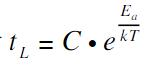 Where C is a constant; EA is the activation energy of chemical reaction. The first mock exam AF based on this model is:
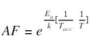 Here, TACC is the temperature under acceleration.
(2) Erin model:Compared with Arrhenius model, Erin model can consider the influence of more types of stresses other than temperature, and potentially consider the interaction between these different types of stresses.
_20210823134614_446.jpg)
4. Failure analysis technology
Failure analysis technology is the means and method used in failure analysis theory. It mainly includes six aspects: failure location technology; Sample preparation technology; Microanalysis technology; Stress verification technology; Electronic analysis technology; Component analysis technology.
1. Failure location technology
The main purpose of failure location technology is to determine the failure location of the detection target. With the complexity of modern integrated circuits and electronic components, failure location technology is particularly important. There are many methods for failure location technology, among which X-ray, Sam and other nondestructive testing can be carried out without opening. X-ray can be used to observe the internal structure of components and multilayer printed circuit boards, open or short circuit of internal leads, bonding defects, solder joint defects, packaging cracks, holes, bridges, steles and missing devices. Sam can observe internal cracks, delamination defects, cavities, bubbles, voids, etc. If X-ray and Sam cannot detect the failure part, the components need to be unsealed, and then the failure can be located by other methods, such as microscopic inspection.
2. Sample preparation technology
To solve most failure analysis, anatomical analysis technology is needed, that is, cross-sectional analysis of samples, which does not damage the observation and test parts. The sample preparation steps generally include: opening the package, removing the passivation layer, and removing the interlayer medium for multilayer chip. Mechanical or chemical opening methods can be used to open the package. The passivation layer can be removed by chemical corrosion or plasma corrosion (such as ICP, RIE), FIB, etc.
3. Microanalysis technique
Microscopic analysis technology is used to analyze the failure cause, determine the failure mechanism and locate the failure mentioned above. Various microscopes are generally used for microscopic analysis, and they have their own advantages and disadvantages, such as stereomicroscope with large depth of view and strong three-dimensional imaging; Metallographic microscope with good plane imaging effect and prominent color; SEM with high magnification (up to hundreds of thousands of times); TEM with high sample preparation requirements and observable lattice structure; Infrared microscope with low imaging accuracy but convenient operation; For the optical radiation microscope with high imaging accuracy, the equipment and methods should be selected according to the actual situation.
4. Stress verification technology
There are differences in the reliability of electronic components in different environments, such as stress under different humidity and temperature, electrical stress under different current and voltage, which will lead to changes in the performance of electronic components or failure. Therefore, various environmental parameters can be simulated to verify the reliability of components under various stresses.
5. Electronic analysis technology
There are many methods of failure analysis using electronic, such as EBT, EPMA, SEM, TEM, AES, etc.
6. Component analysis technology
It is necessary to determine the composition and composition of a part of the components, that is, it is necessary to use component analysis technology to judge whether there is pollution or whether the components are correct, which affects the performance of the components. Common equipment include EDS, EDAX, AES, Sims, etc.
Failure occurs in development, production, engineering and other stages, and the collection department of failure information also exists in multiple departments accordingly. If the failure information is not fed back to the failure analysis department in time, the timeliness of failure analysis and the accuracy of analysis results will be affected. Therefore, effective feedback channels must be established to enable failure analysis engineers to timely understand the failure of devices and analysis progress.


