


 Weixin Service

 DouYin
 KuaiShou

What are the general processes of chip testing?
Date:2021-09-16 15:32:07 Views:13621
The purpose of chip testing is to eliminate failure and potential failure chips in the process of design and production and prevent defective products from flowing into customers. Therefore, we need to increase the evaluation of chip test level when selecting the type. Through the communication with the original factory and the sealing and testing factory, we can obtain the key parameters and indicators in the stage of chip design verification → process inspection → wafer test → chip finished product test for comprehensive evaluation.
According to different testing stages, the chip testing process can be divided into three categories: wafer testing, packaging testing and system level testing.
Wafer test (CP)
Wafer testing, also known as CP (chipprobe, which may be called a little differently), is to directly put a whole wafer into the machine for testing. Similar to the following figure.
_20210916152345_922.jpeg)
The wafer to be tested is placed on the support (not actually called the support, it can be understood easily), and the probecard (commonly known as the pin card) is fixed on it. During the test, all test programs are transmitted to the wafer through the probecard. After testing one chip, the bracket will move (the probecard is fixed) and continue to test another chip.
Let's talk about probecard again. It looks like this. The first picture is an overall picture, and the second picture is an enlarged picture of the middle part (source network).

There are many circuits and copper wires on the whole probecard, which can be simply understood as that the testing machine adds the voltage to be tested to the pin of probecard, then stabilizes and converts through the circuit inside, and finally transmits it to the silver pin in the middle of the second figure. Then pierce the pins of the chip through these very, very thin pins (note that at this time, the chip has not been encapsulated, so there are no pins, only pads, which can be said that these probes are pierced into pads). So in this way, the machine adds the required test voltage to the chip for test.
Wafer testing is generally conducted many times, such as testing the basic functions at room temperature (commonly known as CP1 or sort1), testing again after baking at high temperature (commonly known as CP2), and testing again under the conditions desired by the customer (CP3). Of course, these sequences are different in each family, but the process is the same. Some small problems can't afford the cost of testing, so CP2 and CP3 will be omitted Only CP1 Of course, there are also some small problems. In order to save money, we don't measure CP. Get wafer, cut it directly into each chip, package it, and then test it.
Encapsulation test (finaltest)
After the wafer test, the good chips are marked on the wafer (also known as bluetape), and then cut into individual chips. These chips are packaged into black boxes one by one, which is what it looks like.
_20210916152501_793.jpeg)
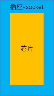
Then we put a pile of black box chips into the socket, and then put the socket into a board.
First of all, we should know that probecard is not required in FT test. How do you test it? After packaging, get the black box chip of the above figure. It can be seen that there are many silver metal pins on it. At this time, it must be impossible to use the probecard at the CP end. The best way is to find a socket, insert these chips with pins into the socket, and then supply power to the socket. Ah, this socket is called socket, so add voltage and current directly to the socket.
Another problem here is that such a test is too slow. It's best to put these sockets together. Then the test efficiency is greatly improved. So we put these sockets on a board, which is called board. What is the relationship between socket and board? Look at the picture below.
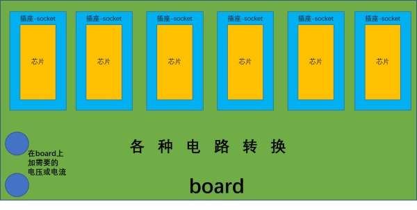
During the test, put the board on the testing machine, and the testing machine will add the required voltage and current to the interface on the board, and then add these voltage and current to the socket through the circuit on the board, and the socket will add the voltage and current to the chip. This is the general flow of FT test.
If you don't understand it, take a look at the power plug-in. The main power line is the testing machine. The plug-in is the board. Each socket on the plug-in is the socket. Plug the electrical appliance into the socket, and the electrical appliance is the chip.
Finally, mark the test results, and then send the good chip to fabless.
System level test
The test factory will package the chips that have passed the test and send them to fabless. After fabless gets the chips, it will install them on the system board, similar to this.
_20210916152709_220.jpg)
Then test the corresponding functions on the system board to see if the chip can meet the required parameters. This is system level testing. Most system level tests are sampling tests. In fact, if there are bad chips at this stage, the consequences will be very serious, because I don't know how many products have problems, so I can't assess the impact.
The above is the related content of the "chip test process" brought by the core creation test. Through this article, I hope it can be helpful to you. If you like this article, you might as well continue to pay attention to our website, and we will bring more wonderful content later. If you have any needs related to the inspection and testing of electronic products, please call Chuangxin testing, and we will serve you wholeheartedly.


