Talk about the professional visual inspection company for chip appearance defect inspection
Date:2021-09-24 14:25:00 Views:3686
With the continuous upgrading of artificial intelligence technology, product appearance defect detection can also be realized through artificial intelligence technology. Due to the disadvantages of slow detection efficiency and low detection accuracy in traditional artificial detection, visual detection of surface appearance defects can better replace traditional detection methods. At each node, the feature size of the chip becomes smaller and smaller, and the defects are more difficult to find. Defects are undesirable deviations in the chip, which will affect the yield and performance. The advantages of non-contact, continuity, economy and flexibility of machine vision detection make people have a better choice. Manual detection is gradually replaced by machine vision detection. The application of machine vision detection system to semiconductor detection is mainly through positioning the real-time captured image by pattern matching, analyzing and processing the image and obtaining various parameters of the image, Compare and calculate with the preset detection standard, and then judge whether the image is qualified or not.
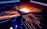
According to different application scenarios, chips can be divided into civil grade (consumer grade), industrial grade, automotive grade and military grade chips. Their main difference is in the working temperature range. Due to the complex war environment, the electronic components used in military grade chips should be sufficiently resistant to operation. For example, the electronic components in missiles, satellites, tanks and aircraft carriers are the most advanced. They are 10 years ahead of the industrial grade and about 20 years ahead of the commercial grade. The most expensive and precise components are reflected in the military grade, Its working temperature is - 55 ℃ ~ + 150 ℃; Working temperature range of automotive chip - 40 ℃ ~ + 125 ℃; The industrial grade chip is slightly lower than the automobile grade, the price is the second, the precision is the second, and the working temperature range is - 40 ℃ ~ + 85 ℃; Civil / consumer chips are the kind traded in the market. Computers and mobile phones are basically commercial.
_20210924142338_256.jpg)
Industrial vision has four main application categories: measurement, positioning, detection and recognition. In recent years, with the maturity of artificial intelligence and other technologies, industrial vision has developed rapidly, which can effectively improve the yield and production efficiency, reduce labor costs and reduce the naked eye injury of quality inspectors. Among them, industrial visual inspection is divided into surface quality inspection and visual positioning (binocular and multi eye positioning), which is mainly applied to the inspection of scratches, dirt, bright spots, missing corners and bulges of mechanical parts.
Chip appearance defects mainly include:
1. Package defect;
2. Printing defects;
3. Pin defect.
Main inspection contents of chip appearance defect inspection:
1. The contents of package inspection include scratch, stain, damage, underfilling, overflow, etc.
2. The contents of printing inspection include: misprint, offset, missing print, overprint, blur, tilt, displacement, hyphenation, double-layer printing, no word mold, etc.
3. The contents of pin detection include: pin missing, pin damaged, pin spacing, pin width, pin bending, pin span, pin length difference, pin standing height and pin coplanarDegree, pin inclination, etc.
The above is the related content of "chip appearance defect detection". In the current industrial market, there are many kinds of chips, and they are increasing. The output of each kind of chip ranges from thousands to tens of thousands. The appearance defect detection system can obtain the surface image of the product according to the lens light source, carry out a series of operations such as accurate positioning, resolution and defect classification for the product image, and deal with and solve the existing problems in time.


 Weixin Service

 DouYin

 KuaiShou


