


 Weixin Service

 DouYin
 KuaiShou

Detailed explanation of knowledge points of MOS tube (FET) failure analysis
Date:2022-01-10 13:47:26 Views:6056
As a voltage driven high current device, MOS transistor is widely used in circuits, especially in power systems. MOS transistor has some characteristics that we should pay special attention to in practical applications.
MOS tube body diode, also known as parasitic diode, exists in a single MOS tube device, but not in integrated circuit lithography. This diode can play the role of reverse protection and freewheeling when driven by high current and inductive load. Generally, the forward conduction voltage drop is about 0.7 ~ 1V. Because of the existence of this diode, MOS devices can not simply see the role of a switch in the circuit, For example, in the charging circuit, after the charging is completed and the power supply is removed, the battery will supply power to the outside in reverse, which is usually a result we don't want to see. The general solution is to add a diode to prevent reverse power supply. Although this can be done, the characteristics of the diode determine that there must be a forward voltage drop of 0.6 ~ 1V, which causes serious heating under high current, At the same time, it causes waste of energy and low energy efficiency of the whole machine. Another method is to add a back-to-back MOS tube, which uses the low on resistance of MOS tube to achieve the purpose of energy saving. Another common application of this feature is low-voltage synchronous rectification.
MOS failure reason:
1. Avalanche failure (voltage failure)That is, we often say that the bvdss voltage between drain and source exceeds the rated voltage of MOSFET and reaches a certain capacity, resulting in MOSFET failure.
2. SOA failure (current failure)That is, failure caused by exceeding the safe working area of MOSFET is divided into failure caused by ID exceeding the device specification and failure caused by excessive ID and excessive loss and long-term heat accumulation of the device.
3. Body diode failure: in bridge, LLC and other topologies where the body diode is used for freewheeling, the failure caused by the destruction of the body diode.
4. Resonance failure: in the process of parallel use, the grid and circuit parasitic parameters lead to the failure caused by oscillation.
5. Electrostatic failure: device failure caused by static electricity of human body and equipment in autumn and winter.
6. Grid voltage failure: the gate oxygen layer fails because the gate suffers an abnormal voltage spike.
The specific analysis is as follows:
1) Avalanche failure analysis (voltage failure)
What is avalanche failure? In short, it is a failure mode of MOSFET on the power board due to the superposition of bus voltage, transformer reflection voltage, leakage inductance peak voltage and other system voltages between MOSFET drain sources. In short, it is a common failure mode caused by the MOSFET drain source voltage exceeding its specified voltage value and reaching a certain energy limit.
The following picture is the equivalent schematic diagram of avalanche test, which can be understood by power engineers.
失效分析知识点详解")
Maybe we often ask device manufacturers to conduct failure analysis on MOSFETs on our power board. Most manufacturers only give an EAS EOS and other conclusions, so how can we distinguish whether it is avalanche failure? The following is a device diagram after avalanche test failure. We can compare it to determine whether it is avalanche failure.
Preventive measures for avalanche failure
In the final analysis, avalanche failure is voltage failure, so we focus on voltage. For details, refer to the following methods.
1: Reasonable derating use. At present, 80% - 95% derating is generally selected for derating in the industry. The specific situation is selected according to the warranty terms and circuit concerns of the enterprise.
2: Reasonable transformer reflection voltage.
3: Reasonable RCD and TVs absorption circuit design.
4: Thick and short layout structure shall be adopted for high current wiring to minimize parasitic inductance.
5: Select a reasonable grid resistance Rg.
6: In high-power power supply, RC damping or zener diode can be added as needed for absorption.
2) SOA failure (current failure)
To put it simply, the second point is SOA failure
SOA failure refers to the failure mode caused by instantaneous local heating when the abnormal high current and voltage of the power supply are superimposed on the MOSFET at the same time. Or the thermal breakdown mode caused by the chip, radiator and package can not reach the thermal balance in time, resulting in heat accumulation, and the continuous heating makes the temperature exceed the limit of oxide layer.
For the parameter limit values of SOA lines, please refer to the following pictures
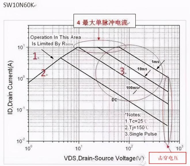
1: Limited by maximum rated current and pulse current
2: RDSON limited to maximum temperature savings.
3: Limited by the maximum dissipation power of the device.
4: Limited by the maximum single pulse current.
5: Breakdown voltage bvdss limit zone
The MOSFET on our power supply can effectively avoid the power failure caused by MOSFET as long as the device is within the upper limit area.
Preventive measures against SOA failure
1: Ensure that all power limits of MOSFET are within the SOA limit line under the worst condition.
2: The OCP function must be precise and detailed.
When designing OCP points, most engineers may take 1.1-1.5 times the current margin, and then start debugging RSENSE resistance according to the protection voltage of IC, such as 0.7V.
Some experienced people will take into account the actual impact of detection delay time and CISS on OCP.
However, there is a more noteworthy parameter at this time, that is, TD (off) of MOSFET.
What effect does it have? Let's look at the flyback current waveform below.

It can be seen from the figure that when the current waveform approaches the current peak, there is a drop, and there is a rise time after this drop point. The essence of this time is that after the IC detects the overcurrent signal and turns off, the MOSFET itself also starts to turn off. However, due to the turn-off delay of the device itself, the current will have a secondary rise platform. If the secondary rise platform is too large, Then, when the residual design of the transformer is insufficient, it is very likely to produce a current shock of magnetic saturation or a failure of current exceeding the device specification.
3: There is not much to say about reasonable thermal design margin. Each enterprise has its own derating specifications, which can be strictly implemented. If not, add radiators.
3) Body diode failure
MOSFETs have different roles in different topologies and circuits. For example, in LLC, the speed of diodes in the body is also an important factor in the reliability of MOSFETs. It is difficult to distinguish between bulk diode failure and drain source voltage failure, because the diode itself is a parasitic parameter. Although it is difficult to distinguish the physical causes after failure, there are great differences in the solutions to prevent voltage and diode failure, which are mainly analyzed in combination with their own circuits.
Failure prevention measures of body diode
In fact, the body diode is not in the way most of the time, and sometimes it has advantages. For example, it is used on the H bridge to save diodes. Of course, when there are obstacles, it is OK to use two MOS tube heads head to head or tail to tail in series.
The diode is determined by the process. Don't care too much. Just accept its existence. In addition, to say a few more words, in fact, the D and s of MOS transistors are essentially symmetrical structures, just two contacts of the channel. However, since the opening and closing of the channel involves the electric field between the gate and the substrate, it is necessary to give the substrate a certain potential. Because MOS has only three pins, it is necessary to connect the substrate to one of the other two pins. Then the pin connected to the substrate is s, and the pin not connected to the substrate is d. when we apply, the potential of S is often stable. In integrated circuits, such as CMOS or analog switches, because the chip itself has power pins, the substrate of those MOS tubes is not connected with the pins, but directly connected to the VCC or Vee of the power supply. At this time, D and s have no difference.
4) Resonance failure
Parasitic gate oscillation that occurs when a power MOS FET is connected directly without a gate resistor inserted in parallel. When the drain source voltage is repeatedly turned on and off at high speed, this parasitic oscillation occurs on the resonant circuit formed by the gate drain capacitance CGD (CRSs) and the gate pin inductance LG. When resonance condition( ω L=1/ ω C) When it is established, a vibration voltage far greater than the driving voltage VGS (in) is applied between the grid and the source. The grid is damaged due to exceeding the rated voltage between the grid and the source, or the vibration voltage when turning on and off the drain source voltage causes positive feedback through the overlap of grid drain capacitance CGD and VGS waveforms. Therefore, oscillation damage may be caused by misoperation.
Preventive measures for resonance failure
Resistance can suppress oscillation because of damping. However, a small resistance connected in series with the grid does not solve the problem of oscillation damping It is mainly the reason for the impedance matching of the driving circuit and the reason for adjusting the switching time of the power tube.
5) Electrostatic failure
The basic physical characteristics of static electricity are: attraction or repulsion; There is electric field and potential difference with the earth; Discharge current will be generated. These three situations will have the following effects on electronic components:
1. Components absorb dust, change the impedance between lines, and affect the function and service life of components.
2. The insulating layer and conductor of the element are damaged by electric field or current, so that the element cannot work (completely damaged).
3. The component is injured due to instantaneous electric field soft breakdown or current overheating. Although it can still work, its service life is damaged.
Preventive measures for electrostatic failure
The current tolerance of the protection diode at the input end of MOS circuit is generally 1mA. When excessive transient input current (more than 10mA) may occur, the input protection resistance shall be connected in series. The protective resistance was not added in the initial design, so this is also the reason for the possible breakdown of MOS tube. This failure can be prevented by replacing a MOS tube with protective resistance inside. In addition, because the instantaneous energy absorbed by the protection circuit is limited, too large instantaneous signal and too high electrostatic voltage will make the protection circuit ineffective. Therefore, the electric soldering iron must be reliably grounded during welding to prevent leakage and electric shock through the input end of the device. Generally, when in use, the waste heat of the electric soldering iron can be used for welding after power failure, and its grounding pin shall be welded first.
6) Grid voltage failure
There are three main sources of abnormal high voltage of Grid:
1: Static electricity during production, transportation and assembly.
2: High voltage resonance caused by parasitic parameters of devices and circuits when the power supply system works.
3: In case of high voltage impulse, the high voltage is transmitted to the grid through GGD (failure caused by this reason is more common in lightning test).
As for PCB pollution level, electrical gap and other phenomena such as entering the grid after high voltage breakdown IC, there will be no too much explanation.
Preventive measures for grid voltage failure
Overvoltage protection between gate and source: if the impedance between gate and source is too high, the sudden change of drain source voltage will be coupled to the gate through inter electrode capacitance, resulting in quite high UGS voltage overshoot. This voltage will cause permanent damage to the gate oxide layer. If the UGS transient voltage in the positive direction will also lead to misoperation of the device. Therefore, the impedance of the grid driving circuit should be properly reduced, and the damping resistance or voltage stabilizing tube with a voltage stabilizing value of about 20V should be connected between the grid and the source. Special attention shall be paid to prevent open grid operation. The second is overvoltage protection between drains. If there is inductive load in the circuit, when the device is turned off, the sudden change of drain current (di / DT) will produce much higher drain voltage overshoot than the power supply voltage, resulting in device damage. Protective measures such as voltage stabilizing tube clamping, RC clamping or RC suppression circuit shall be taken.
In addition, MOSFET damage is mainly caused by use / quality and process Use:
1) Static electricity is damaged. At the beginning, it may be switched on and off like a good pipe. After a period of time, it will fail to blow up the machine and GDS will be fully short circuited
2) Space plasma damage, light and electrostatic damage, heavy direct GDS short circuit Everyone should pay attention! Do not use negative ion generator or air conditioner with this function where MOSFET or IGBT / COMS devices are placed!
3) Leakage damage. In most cases, GDS is fully short circuited, and DS or GD will be open circuited in some cases
4) Overdrive: after the driving voltage exceeds 18V, the GDS will be completely disconnected after a period of use
5) When the negative pressure is closed and the gate is added with negative pressure, the anti noise ability of MOSFET is strengthened, but the withstand voltage ability of DS decreases. Improper negative pressure will lead to insufficient withstand voltage of DS, breakdown damage and short circuit of GDS
6) The grid parasitic induced negative pressure is damaged, which is the same as the improper negative pressure drive, but the negative pressure is not artificially added. It is due to the parasitic LC induction of the line, which induces and generates a negative pulse on the deletion.
The above is the content related to the failure analysis of MOS tube (field effect tube) compiled by the core detection team. I hope it will be helpful to you. Chuangxin testing is a professional testing organization for electronic components. At present, it mainly provides integrated circuit testing services such as capacitance, resistance, connector, MCU, CPLD, FPGA and DSP. Specializing in functional testing of electronic components, incoming appearance testing of electronic components, anatomical testing of electronic components, acetone testing, X-ray scanning testing of electronic components and RoHS component analysis testing. Welcome to call, we will serve you wholeheartedly!


