Cause analysis and solution of electrostatic breakdown of MOS tube
Date:2022-01-10 13:35:00 Views:3780
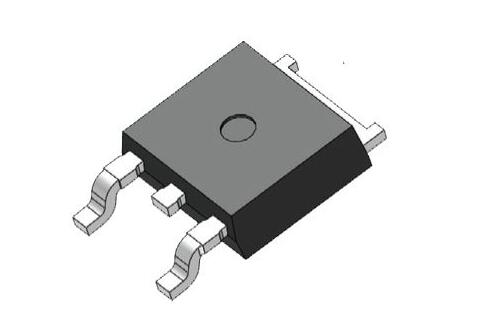
MOS transistor is a metal oxide semiconductor field effect transistor, which belongs to insulated gate type.Why is MOS tube broken down by static electricity? Does electrostatic breakdown refer to the insulating layer that breaks down the G pole of MOS tube? Must a breakdown be a short circuit? What about JFET tube electrostatic breakdown?
MOS tube is an ESD sensitive device. Its input resistance is very high, and the capacitance between gate and source is very small, so it is very easy to be charged by external electromagnetic field or electrostatic induction (a small amount of charge may form a very high voltage on the inter electrode capacitance (think u = q / C) and damage the tube). Moreover, it is difficult to discharge charge in strong electrostatic occasions, which is easy to cause electrostatic breakdown. There are two ways of electrostatic breakdown: one is voltage type, that is, the thin oxide layer of the grid breaks down and forms a pinhole to short circuit between the grid and the source, or between the grid and the drain; The second is the power type, that is, the metallized film aluminum strip is fused, resulting in open grid or open source. JFET tube, like MOS tube, has high input resistance, but the input resistance of MOS tube is higher.
Electrostatic discharge forms a short-time high current, and the time constant of discharge pulse is much less than that of device heat dissipation. Therefore, when the electrostatic discharge current passes through the PN junction or Schottky junction with a small area, it will produce a large instantaneous power density and form local overheating, which may make the local junction temperature reach or even exceed the intrinsic temperature of the material (such as the melting point of silicon 1415 ℃), make the junction area melt locally or at many places, resulting in short circuit of PN junction and complete failure of the device. The occurrence of this failure mainly depends on the power density in the internal area of the device. The smaller the power density, the less vulnerable the device is to damage.
The reverse biased PN junction is more prone to thermal failure than the positive biased PN junction. The energy required to damage the junction under the reverse biased condition is only about one tenth of that under the positive biased condition. This is because during reverse bias, most of the power is consumed in the center of the junction, while during positive bias, it is mostly consumed in the body resistance outside the junction. For bipolar devices, the area of the emitter junction is usually smaller than that of other junctions, and the junction surface is closer to the surface than other junctions, so the degradation of the emitter junction is often observed. In addition, PN junction with breakdown voltage higher than 100V or leakage current less than 1NA (such as gate junction of JFET) is more sensitive to electrostatic discharge than conventional PN junction with similar size.

All things are relative, not absolute. MOS tube is just more sensitive than other devices. ESD has a great feature of randomness. It can not be broken down without touching MOS tube. In addition, even if ESD is generated, it does not necessarily break down the pipe. The basic physical characteristics of static electricity are: (1) it has the force of attraction or repulsion; (2) There is electric field and potential difference with the earth; (3) Discharge current will be generated. These three situations, namely ESD, will generally affect electronic components in the following three situations: (1) components absorb dust, change the impedance between lines, and affect the function and service life of components; (2) The insulating layer and conductor of the element are damaged by electric field or current, so that the element cannot work (completely damaged); (3) The component is injured due to instantaneous electric field soft breakdown or current overheating. Although it can still work, its service life is damaged. Therefore, the damage of ESD to MOS tube may be one or three cases, not necessarily the second case every time. In the above three cases, if the components are completely damaged, they will be detected and eliminated in production and quality test, with less impact. If the component is slightly damaged, it is not easy to be found in the normal test. In this case, it is often found to be damaged after repeated processing or even when it is in use. Not only is it difficult to check, but also the loss is difficult to predict. The harm of static electricity to electronic components is no less than the loss of serious fire and explosion accidents.
Under what circumstances will electronic components and products be damaged by static electricity? It can be said that the whole process of electronic products from production to use is threatened by electrostatic damage. From device manufacturing to plug-in assembly and welding, whole machine assembly, packaging and transportation to product application, they are all under the threat of static electricity. In the whole production process of electronic products, at every small step in every stage, electrostatic sensitive components may be affected or damaged by static electricity. In fact, the most important and easily neglected point is in the process of component transmission and transportation. In this process, transportation is easily exposed to static electricity generated by external electric field (such as passing near high-voltage equipment, frequent movement of workers, rapid movement of vehicles, etc.), so special attention should be paid to the transmission and transportation process to reduce losses and avoid indifferent disputes. In case of protection, add Zener regulator for protection.
Nowadays, MOS transistors are not so easy to be broken down, especially high-power VMOS. Many of them are protected by diodes. VMOS has large gate capacitance and can not induce high voltage. Different from the dry north, the south is wet and not easy to generate static electricity. In addition, IO port protection has been added to most CMOS devices. However, it is not a good habit to directly contact CMOS device pins by hand. At least make the solderability of pins worse.
Cause and solution of MOS tube breakdown
The input resistance of the first MOS tube itself is very high, and the capacitance between the gate and source is very small, so it is very easy to be charged by the induction of external electromagnetic field or static electricity, and a small amount of charge can form a very high voltage (U = q / C) on the inter electrode capacitance and damage the tube. Although the MOS input terminal has anti-static protection measures, it still needs to be treated with care. It is best to use metal containers or conductive materials for packaging in storage and transportation, and do not put it in chemical materials or chemical fiber fabrics that are prone to electrostatic high voltage. During assembly and commissioning, tools, instruments and worktables shall be well grounded. To prevent damage caused by electrostatic interference of operators, if nylon and chemical fiber clothes are not suitable, it is best to ground hands or tools before contacting the manifold block. When straightening, bending or manual welding of device leads, the equipment used must be well grounded.
The current tolerance of the protection diode at the input end of the second MOS circuit is generally 1mA when it is turned on. When excessive transient input current (more than 10mA) may occur, the input protection resistance shall be connected in series. Therefore, a MOS tube with internal protective resistance can be selected for application. In addition, because the instantaneous energy absorbed by the protection circuit is limited, too large instantaneous signal and too high electrostatic voltage will make the protection circuit ineffective. Therefore, the electric soldering iron must be reliably grounded during welding to prevent leakage and electric shock through the input end of the device. Generally, when in use, the waste heat of the electric soldering iron can be used for welding after power failure, and its grounding pin shall be welded first.
MOS is a voltage driving element and is very sensitive to voltage. The suspended G is easy to accept external interference to turn on the MOS. The external interference signal charges the G-S junction capacitor. This small charge can be stored for a long time. In the test, G is dangerously suspended. Many tubes burst because of this. G is connected to a pull-down resistor to the ground, and the bypass interference signal will not be directly connected. Generally, it can be 10 ~ 20K. This resistance is called gate resistance. Its function is 1: to provide bias voltage for FET; Function 2: play the role of discharge resistance (protect grid G ~ source s). The first function is easy to understand. Here we explain the principle of the second function: the resistance between the G-S electrodes of the protection grid G ~ source s: FET is very large, so as long as there is a small amount of static electricity, a high voltage can be generated at both ends of the equivalent capacitance between his G-S electrodes. If these small amounts of static electricity are not discharged in time, The high voltage at both ends may cause misoperation of the FET and even breakdown of its G-S electrode; At this time, the resistance added between the grid and the source can discharge the above static electricity, so as to protect the FET.
MOS tube electrostatic breakdown has the following characteristics about through breakdown
1. The breakdown point of through breakdown is soft, and the current increases gradually in the process of breakdown, which is due to the wide expansion of depletion layer and large current. On the other hand, the wide depletion layer is prone to dibl effect, which makes the positive bias of the source substrate junction show the characteristics of gradually increasing current.
2. The soft breakdown point of through breakdown occurs when the depletion layer of the source and drain is connected. At this moment, the carrier at the source end is injected into the depletion layer and accelerated by the electric field in the depletion layer to reach the drain end. Therefore, the current of through breakdown also has a sharp increase point, which is different from the sharp increase of current during avalanche breakdown, The current at this time is equivalent to the current when the source substrate PN junction is conducting, and the current during avalanche breakdown is mainly the avalanche current during PN junction reverse breakdown. If current limitation is not made, the avalanche breakdown current will be large.
3. Through breakdown generally does not show destructive breakdown. Because the penetration breakdown field strength does not reach the avalanche breakdown field strength, many electron hole pairs will not occur.
4. The penetration and breakdown generally occur in the channel body, and the channel surface is not easy to penetrate. This is mainly because the channel injection makes the surface concentration higher than the concentration. Therefore, there is generally anti penetration injection for NMOS tubes.
5. Generally, the concentration at the edge of the beak is greater than that at the center of the channel, so the through breakdown usually occurs in the center of the channel.
6. The length of polycrystalline gate has an effect on the through breakdown. With the increase of gate length, the breakdown increases. Strictly speaking, it also has an impact on avalanche breakdown, but it is not so obvious.
The above is the related content of "MOS tube is electrostatic breakdown" brought by the core detection. Through this article, I hope it can be helpful to you. If you like this article, you might as well continue to pay attention to our website, and we will bring more wonderful content later.


 Weixin Service

 DouYin
 KuaiShou


