Description:Scanning acoustic microscopy (SAM), also denominated acoustic micro imaging (AMI) and scanning acoustic tomography (SAT), is a non-destructive testing method. It utilizes the contrast between images and acoustic waves to analyze the internal layers of specimens, determine defect shapes and sizes, and identify defect orientations. It can also detect the counterfeit detection of surface printing duplication, surface grinding, and re-coating on integrated circuits.
Our Strengths:ChuangXin Testing Center is equipped with a complete range of probes, ranging from low frequencies such as 15MHz, 30MHz, 50MHz, 75MHz, to high frequencies like 100MHz and 230MHz. These probes can meet the testing requirements of integrated circuits and PCB boards with various packaging types such as SOP, DIP, PLCC, TO, QFP, BGA, SOT, QFN, TQFP, DFN, Flip Chip, WLCSP, FCBGA, as well as IGBTs and capacitors and so on.
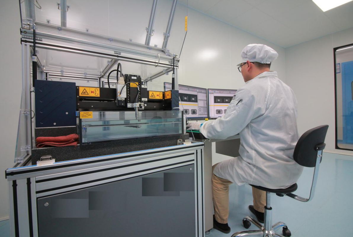
Image of Scanning Acoustic Tomography Equipment:
Case Studies:
1.Abnormal Case in SOP Package:
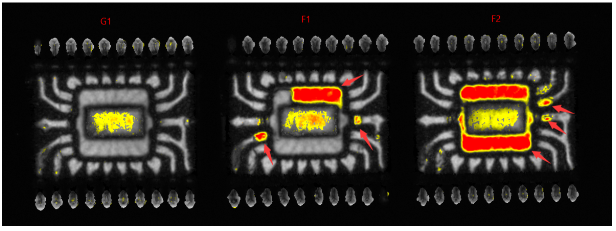
Delamination Anomalies Between Internal Pins, Substrate Surface, and Encapsulation Interface (Reflection-Mode View)
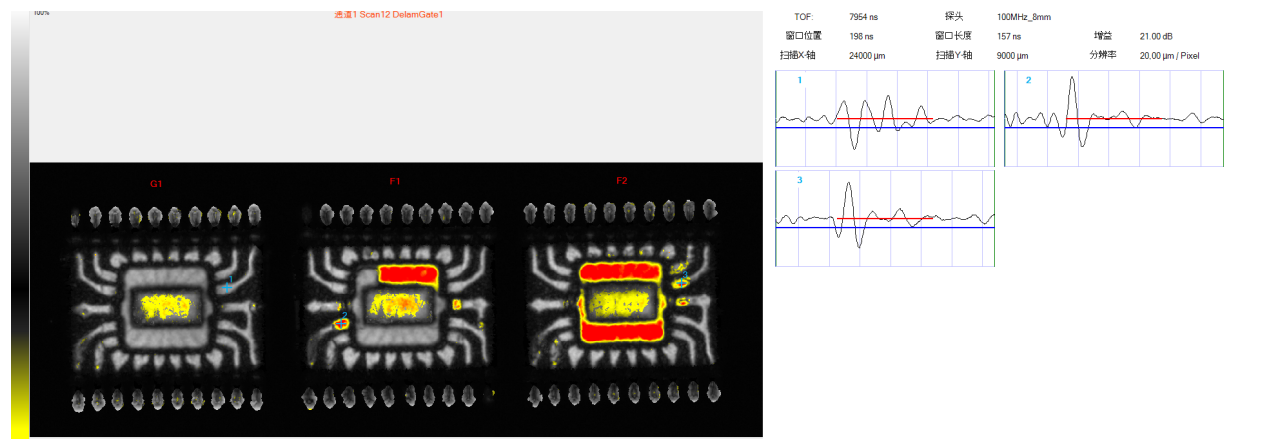
Delamination Anomalies Between Internal Pins, Substrate Surface, and Encapsulation Interface (Reflection-Mode Waveform View)
2. Abnormal Case in TO Package:
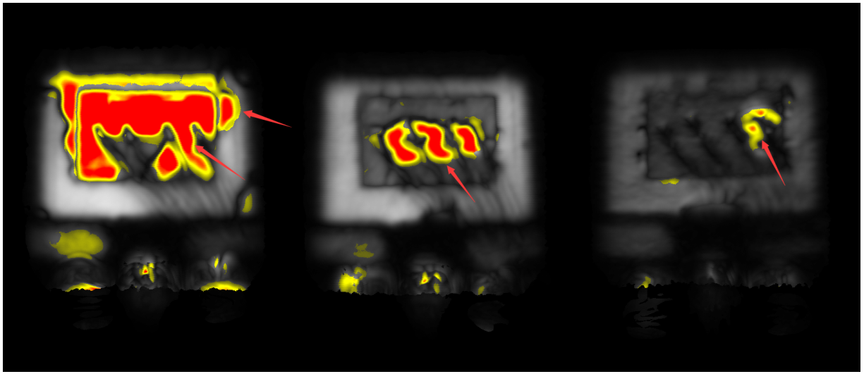
Delamination Anomalies Between Wafer, Substrate Surface, and Encapsulation Interface (Reflection-Mode View)
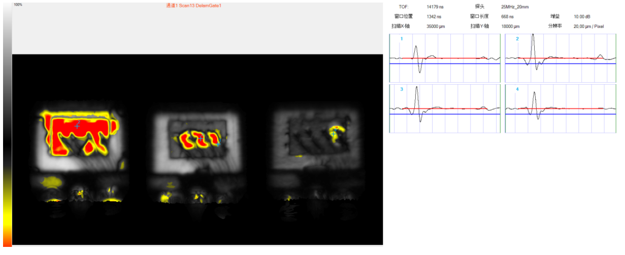
Delamination Anomalies Between Wafer, Substrate Surface, and Encapsulation Interface (Reflection-Mode Waveform View)
3. Abnormal Case in QFP Package:
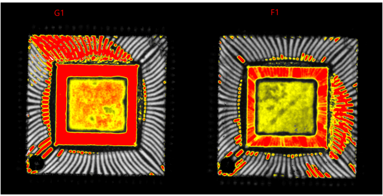
Delamination Anomalies Between Internal Pins, Substrate Surface, and Encapsulation Interface (Reflection-Mode View)
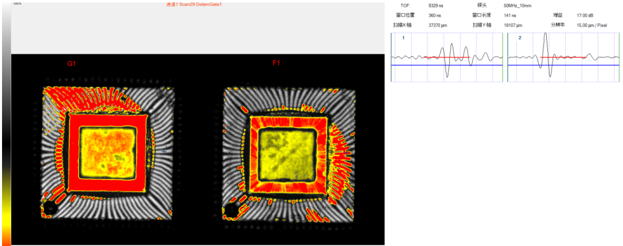
Delamination Anomalies Between Internal Pins, Substrate Surface, and Encapsulation Interface (Reflection-Mode Waveform View)
4. Abnormal Case in Counterfeit Detection:
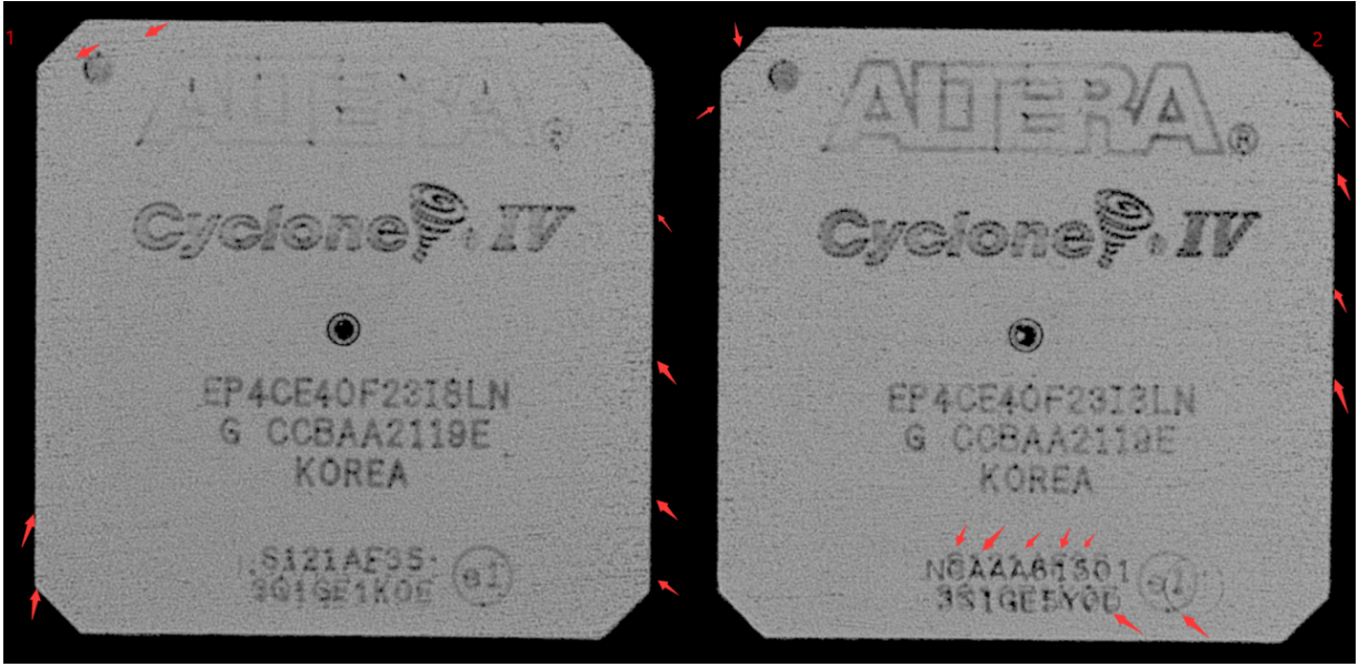
Surface Printing Duplication, Abnormal Edge Grinding Marks (Reflection-Mode View)
5.IGBT Testing Case:
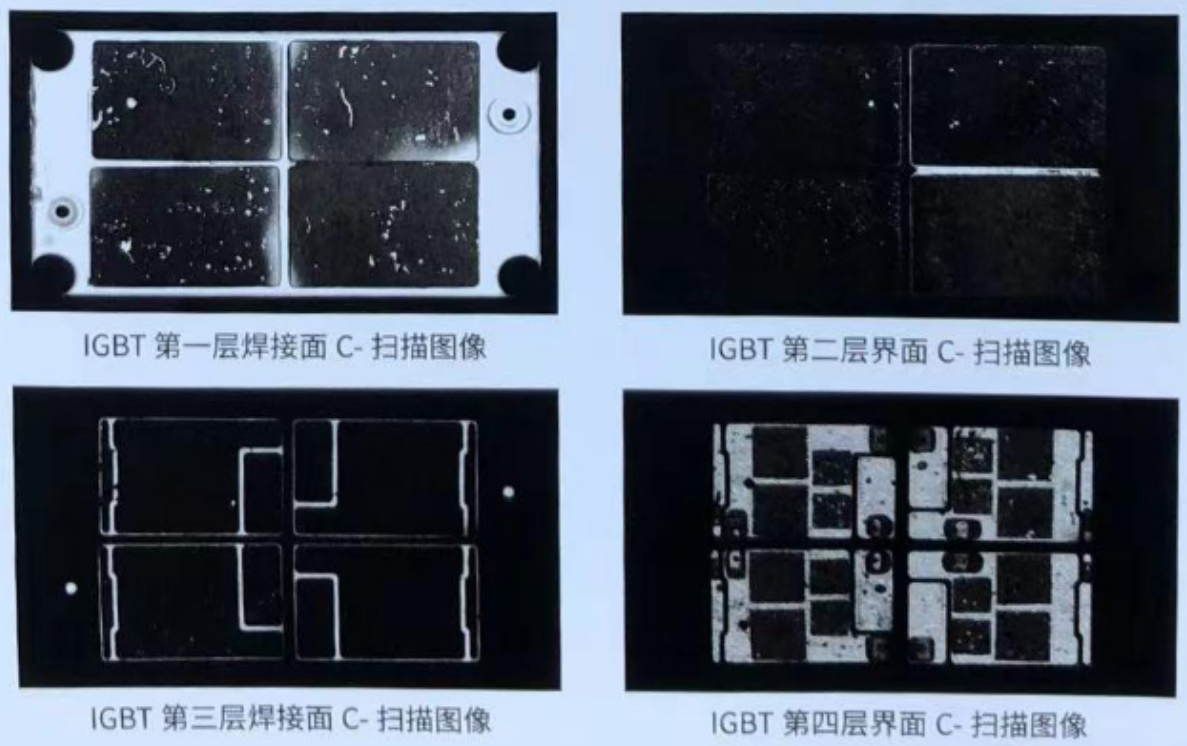

First layer: Solder side between the heat-dissipated copper substrate and the bottom copper-clad layer of the DBC ceramic substrate;
Second layer: Interface between the bottom copper-clad layer of the DBC ceramic substrate and the ceramic;
Third layer: Interface between the ceramic of the DBC ceramic substrate and the upper copper-clad layer;
Fourth layer: Solder side between the upper copper-clad layer of the DBC ceramic substrate and the chip


 Weixin Service

 DouYin
 KuaiShou


