SERVICE

-
IC Counterfeit Detection
- IC Counterfeit Detection-Introduce
-
Non-Destructive Testing (NDT)
-
Destructive Testing
-
Value-Added Services
-
Destructive Physical Analysis (DPA)
- Destructive Physical Analysis (DPA)-Introduce
- External Visual Inspection
- X-Ray inspection
- Functional Testing (FT)
- Particle Impact Noise Detection (PIND/PIN-D)
- Hermeticity
- Internal Water Vapor
- Scanning Acoustic Tomography (SAT Testing)
- Solderability Test
- Decapsulation/Delid Test
- Bond Strength
- Die Shear Strength
- Configuration
-
Failure analysis
- Failure analysis-Introduce
-
Non-Destructive Analysis
-
Electrical Testing
-
Fault Location
-
Destructive Physical Analysis (DPA)
-
Physical Analysis
-
Engineering Sample (ES) Packaging Service
-
Competitor Analysis
-
Development and Functional Verification
- Development and Functional Verification-Introduce
-
New Product Development Testing (FT)
-
Key Functional Testing
-
Materials Analysis
- Materials Analysis-Introduce
-
FIB Circuit Edit
-
Structural Observation
-
Compositional Analysis
- EDS Analysis
-
Reliability Testing
- Reliability Testing-Introduce
-
Reliability Verification of Automotive Integrated Circuits (ICs)
-
Environmental Testing
-
Mechanical Testing
- Pull Test
- Die Strength Test
- High Strain Rate Test - Vibration Test
- Low Strain Rate Test - Bending Test
- High Strain Rate Test - Mechanical Shock Test
- Package Assembly Integrity Test - Wire Bonding Integrity
- Package Assembly Integrity Test
- Combined Vibration/Temperature/Humidity Test
- Combined Temperature/Humidity/Vibration/Altitude Test
- Free Fall Drop Test
- Box Compressive Strength Test
-
Corrosion Testing
-
IP Waterproof/Dust Resistant Test
-
Electromagnetic Compatibility (EMC)
- Electromagnetic Compatibility (EMC)-Introduce
- Immunity to Conducted Disturbances, Induced by Radio Frequency (RF) Fields
- Conducted Immunity Test
- Specific Absorption Rate (SAR) Testing for Electromagnetic Radiation
- Electrical Fast Transient/Burst (EFT/B) Test
- Voltage Flicker/Fluctuation Test
- Voltage Dips, Short Interruptions and Voltage Variations Immunity Test
- Power Frequency Magnetic Field (PFMF) Immunity Test
- Harmonic Interference Test
- Electrostatic Discharge (ESD) Immunity Test
- Surge/Lightning Immunity Test
- Radiated Emissions (RE) Test
- Radio Frequency (RF) Test
-
Chemical Analysis
- Chemical Analysis-Introduce
-
High-Performance Liquid Chromatography (HPLC)
-
Pyrolysis-Gas Chromatography-Mass Spectrometry (PY-GC-MS)
-
Inductively Coupled Plasma Optical Emission Spectroscopy (ICP-OES)
- Flame Retardancy Test
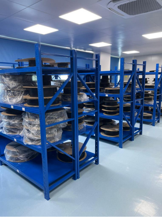
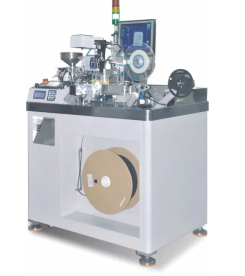
描述: 通过专业半导体编带设备把散装的芯片或者托盘以及管装的样品编成卷带并包装成卷盘,供工厂SMT贴片上机使用。
我们的优势:拥有大量常用规格卷带库存,全自动编带机,超高的编带效率。
编带图片:

全自动编带机:


 Weixin Service

 DouYin
 KuaiShou


