SERVICE

-
IC Counterfeit Detection
- IC Counterfeit Detection-Introduce
-
Non-Destructive Testing (NDT)
-
Destructive Testing
-
Value-Added Services
-
Destructive Physical Analysis (DPA)
- Destructive Physical Analysis (DPA)-Introduce
- External Visual Inspection
- X-Ray inspection
- Functional Testing (FT)
- Particle Impact Noise Detection (PIND/PIN-D)
- Hermeticity
- Internal Water Vapor
- Scanning Acoustic Tomography (SAT Testing)
- Solderability Test
- Decapsulation/Delid Test
- Bond Strength
- Die Shear Strength
- Configuration
-
Failure analysis
- Failure analysis-Introduce
-
Non-Destructive Analysis
-
Electrical Testing
-
Fault Location
-
Destructive Physical Analysis (DPA)
-
Physical Analysis
-
Engineering Sample (ES) Packaging Service
-
Competitor Analysis
-
Development and Functional Verification
- Development and Functional Verification-Introduce
-
New Product Development Testing (FT)
-
Key Functional Testing
-
Materials Analysis
- Materials Analysis-Introduce
-
FIB Circuit Edit
-
Structural Observation
-
Compositional Analysis
- EDS Analysis
-
Reliability Testing
- Reliability Testing-Introduce
-
Reliability Verification of Automotive Integrated Circuits (ICs)
-
Environmental Testing
-
Mechanical Testing
- Pull Test
- Die Strength Test
- High Strain Rate Test - Vibration Test
- Low Strain Rate Test - Bending Test
- High Strain Rate Test - Mechanical Shock Test
- Package Assembly Integrity Test - Wire Bonding Integrity
- Package Assembly Integrity Test
- Combined Vibration/Temperature/Humidity Test
- Combined Temperature/Humidity/Vibration/Altitude Test
- Free Fall Drop Test
- Box Compressive Strength Test
-
Corrosion Testing
-
IP Waterproof/Dust Resistant Test
-
Electromagnetic Compatibility (EMC)
- Electromagnetic Compatibility (EMC)-Introduce
- Immunity to Conducted Disturbances, Induced by Radio Frequency (RF) Fields
- Conducted Immunity Test
- Specific Absorption Rate (SAR) Testing for Electromagnetic Radiation
- Electrical Fast Transient/Burst (EFT/B) Test
- Voltage Flicker/Fluctuation Test
- Voltage Dips, Short Interruptions and Voltage Variations Immunity Test
- Power Frequency Magnetic Field (PFMF) Immunity Test
- Harmonic Interference Test
- Electrostatic Discharge (ESD) Immunity Test
- Surge/Lightning Immunity Test
- Radiated Emissions (RE) Test
- Radio Frequency (RF) Test
-
Chemical Analysis
- Chemical Analysis-Introduce
-
High-Performance Liquid Chromatography (HPLC)
-
Pyrolysis-Gas Chromatography-Mass Spectrometry (PY-GC-MS)
-
Inductively Coupled Plasma Optical Emission Spectroscopy (ICP-OES)
- Flame Retardancy Test
Description:
3D OM (3D Optical Microscope) has advantages such as large depth of field, inclinable angle detection, and advanced measurement capabilities. It can perform on the device under test of different heights at multi angles and obtain clear images for observation. 3D OM is suitable for electronic component solder joint inspection and failure analysis.
Scope of Application:
Detection of part IC package defects, such as appearance integrity, the black gum cracks, pin deformation or discoloration.
Detection of potential PCB defects, such as nodules, weave exposure, glass fiber exposure, solder mask, markings, etc.
Detection of potential detects in electronic products, such as poor soldering.
Solder ball integrity inspection of BGA and flip chip packages, such as ball deformation.
Appearance inspection and analysis of various types of active and passive components.
Analysis and measurement of all semiconductor components.
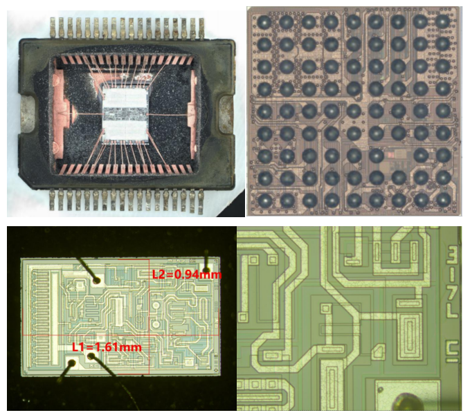
Images of 3D OM Testing:

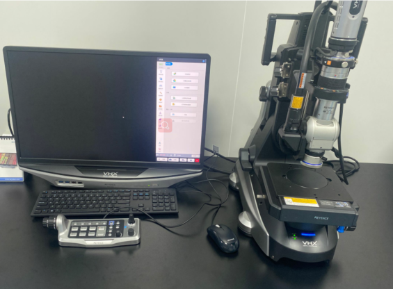
Image of 3D OM Equipment:


 Weixin Service

 DouYin
 KuaiShou


