SERVICE

-
IC Counterfeit Detection
- IC Counterfeit Detection-Introduce
-
Non-Destructive Testing (NDT)
-
Destructive Testing
-
Value-Added Services
-
Destructive Physical Analysis (DPA)
- Destructive Physical Analysis (DPA)-Introduce
- External Visual Inspection
- X-Ray inspection
- Functional Testing (FT)
- Particle Impact Noise Detection (PIND/PIN-D)
- Hermeticity
- Internal Water Vapor
- Scanning Acoustic Tomography (SAT Testing)
- Solderability Test
- Decapsulation/Delid Test
- Bond Strength
- Die Shear Strength
- Configuration
-
Failure analysis
- Failure analysis-Introduce
-
Non-Destructive Analysis
-
Electrical Testing
-
Fault Location
-
Destructive Physical Analysis (DPA)
-
Physical Analysis
-
Engineering Sample (ES) Packaging Service
-
Competitor Analysis
-
Development and Functional Verification
- Development and Functional Verification-Introduce
-
New Product Development Testing (FT)
-
Key Functional Testing
-
Materials Analysis
- Materials Analysis-Introduce
-
FIB Circuit Edit
-
Structural Observation
-
Compositional Analysis
- EDS Analysis
-
Reliability Testing
- Reliability Testing-Introduce
-
Reliability Verification of Automotive Integrated Circuits (ICs)
-
Environmental Testing
-
Mechanical Testing
- Pull Test
- Die Strength Test
- High Strain Rate Test - Vibration Test
- Low Strain Rate Test - Bending Test
- High Strain Rate Test - Mechanical Shock Test
- Package Assembly Integrity Test - Wire Bonding Integrity
- Package Assembly Integrity Test
- Combined Vibration/Temperature/Humidity Test
- Combined Temperature/Humidity/Vibration/Altitude Test
- Free Fall Drop Test
- Box Compressive Strength Test
-
Corrosion Testing
-
IP Waterproof/Dust Resistant Test
-
Electromagnetic Compatibility (EMC)
- Electromagnetic Compatibility (EMC)-Introduce
- Immunity to Conducted Disturbances, Induced by Radio Frequency (RF) Fields
- Conducted Immunity Test
- Specific Absorption Rate (SAR) Testing for Electromagnetic Radiation
- Electrical Fast Transient/Burst (EFT/B) Test
- Voltage Flicker/Fluctuation Test
- Voltage Dips, Short Interruptions and Voltage Variations Immunity Test
- Power Frequency Magnetic Field (PFMF) Immunity Test
- Harmonic Interference Test
- Electrostatic Discharge (ESD) Immunity Test
- Surge/Lightning Immunity Test
- Radiated Emissions (RE) Test
- Radio Frequency (RF) Test
-
Chemical Analysis
- Chemical Analysis-Introduce
-
High-Performance Liquid Chromatography (HPLC)
-
Pyrolysis-Gas Chromatography-Mass Spectrometry (PY-GC-MS)
-
Inductively Coupled Plasma Optical Emission Spectroscopy (ICP-OES)
- Flame Retardancy Test
Description:
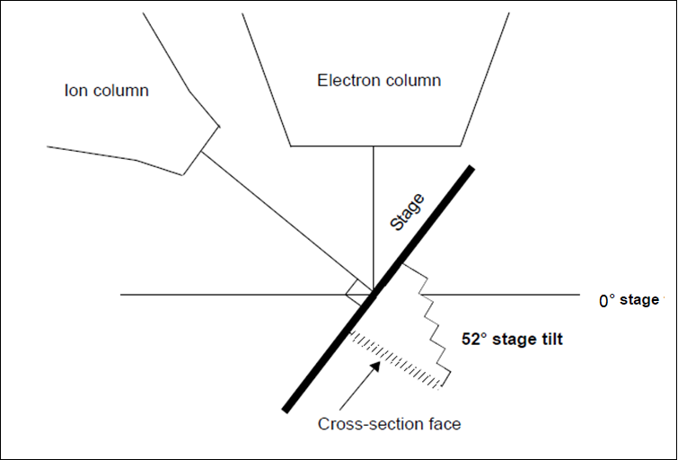
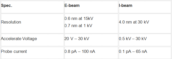
Dual-Beam FIB (Focused Ion Beam) machines use an ion beam to cut samples and an electron beam to observe the cross-section of the sample. They can also perform EDX (Energy Dispersive X-ray) elemental analysis.
Dual-Beam FIB has ultra-high-resolution ion and electron beams, allowing for nanoscale positioning and observation of fine structures in samples. The ion beam can provide a maximum current of up to 65nA, the excellent cutting speed can significantly shorten the analysis time and reduce experimental costs.
Scope of Application:
Failure analysis of semiconductor components and structure analysis (capable of reaching advanced processes down to 14 nm);
Process anomaly analysis in semiconductor production lines;
Analysis of epitaxy and thin film structures;
Preparation of transmission electron microscope (TEM) samples.
Testing Images:
TEM Sample Preparation: TEM specimens with a thickness of approximately 15nm can be prepared using a layer-by-layer delayering technique.

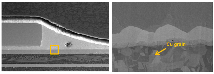
Copper Grain Analysis: By using special sample preparation techniques (grinding + ion milling), a large-area image of copper grains can be quickly obtained.
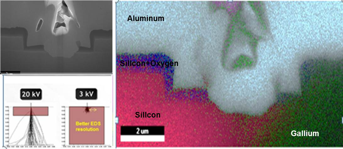
EDS Analysis: Large-area EDS detector (75 mm2) with excellent spatial resolution, is capable of high-end applications involving simultaneous cutting, imaging, and analysis.
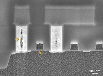
Cross-section Analysis: The Helios NanoLab has excellent E-beam resolution, allowing clear visualization of voids and gate oxide with a resolution as fine as 3nm.
Images of Testing Equipment Energy:
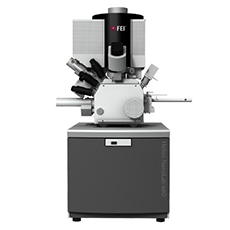
FEI Helios NanoLab 660
Maximum sample size: 150mm;
Equipped with a 75mm2 SDD EDS detector for real-time EDS analysis;
Equipped with MultiChem gas system capable of introducing six types of deposition or stain gases;
When the observation width exceeds 100um or the depth exceeds 50um, it is recommended to switch to Plasma FIB, which has a faster cutting speed.


 Weixin Service

 DouYin
 KuaiShou


