SERVICE

-
IC Counterfeit Detection
- IC Counterfeit Detection-Introduce
-
Non-Destructive Testing (NDT)
-
Destructive Testing
-
Value-Added Services
-
Destructive Physical Analysis (DPA)
- Destructive Physical Analysis (DPA)-Introduce
- External Visual Inspection
- X-Ray inspection
- Functional Testing (FT)
- Particle Impact Noise Detection (PIND/PIN-D)
- Hermeticity
- Internal Water Vapor
- Scanning Acoustic Tomography (SAT Testing)
- Solderability Test
- Decapsulation/Delid Test
- Bond Strength
- Die Shear Strength
- Configuration
-
Failure analysis
- Failure analysis-Introduce
-
Non-Destructive Analysis
-
Electrical Testing
-
Fault Location
-
Destructive Physical Analysis (DPA)
-
Physical Analysis
-
Engineering Sample (ES) Packaging Service
-
Competitor Analysis
-
Development and Functional Verification
- Development and Functional Verification-Introduce
-
New Product Development Testing (FT)
-
Key Functional Testing
-
Materials Analysis
- Materials Analysis-Introduce
-
FIB Circuit Edit
-
Structural Observation
-
Compositional Analysis
- EDS Analysis
-
Reliability Testing
- Reliability Testing-Introduce
-
Reliability Verification of Automotive Integrated Circuits (ICs)
-
Environmental Testing
-
Mechanical Testing
- Pull Test
- Die Strength Test
- High Strain Rate Test - Vibration Test
- Low Strain Rate Test - Bending Test
- High Strain Rate Test - Mechanical Shock Test
- Package Assembly Integrity Test - Wire Bonding Integrity
- Package Assembly Integrity Test
- Combined Vibration/Temperature/Humidity Test
- Combined Temperature/Humidity/Vibration/Altitude Test
- Free Fall Drop Test
- Box Compressive Strength Test
-
Corrosion Testing
-
IP Waterproof/Dust Resistant Test
-
Electromagnetic Compatibility (EMC)
- Electromagnetic Compatibility (EMC)-Introduce
- Immunity to Conducted Disturbances, Induced by Radio Frequency (RF) Fields
- Conducted Immunity Test
- Specific Absorption Rate (SAR) Testing for Electromagnetic Radiation
- Electrical Fast Transient/Burst (EFT/B) Test
- Voltage Flicker/Fluctuation Test
- Voltage Dips, Short Interruptions and Voltage Variations Immunity Test
- Power Frequency Magnetic Field (PFMF) Immunity Test
- Harmonic Interference Test
- Electrostatic Discharge (ESD) Immunity Test
- Surge/Lightning Immunity Test
- Radiated Emissions (RE) Test
- Radio Frequency (RF) Test
-
Chemical Analysis
- Chemical Analysis-Introduce
-
High-Performance Liquid Chromatography (HPLC)
-
Pyrolysis-Gas Chromatography-Mass Spectrometry (PY-GC-MS)
-
Inductively Coupled Plasma Optical Emission Spectroscopy (ICP-OES)
- Flame Retardancy Test
Description:
An IC chip test fixture is designed and fabricated on a PCB test board for the electrical performance testing of integrated circuits. It is used to test various packaged integrated circuit chips, electronic components, CPUs, module core boards, etc.
In the complete chip manufacturing process, chip testing plays a crucial role. Whether it is wafer-level testing before chip dicing or functional electrical testing after packaging, the goal is to identify and improve the yield of defective products. Additionally, before shipping the products, it is necessary to perform relevant reliability verification to estimate the product’s lifespan through accelerated stress tests. Through short-duration high-temperature burn-in, it can identify process defects or early failures, thereby avoiding additional customer return costs. To achieve such conditions and testing environments, it is necessary to plan the test interface before each stage of testing.
Selection of Test Sockets:
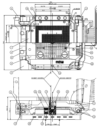
The chip test fixture selects appropriate test sockets based on the chip’s packaging type, shape and size, pitch and number of pins. For example, for testing the BGA2577 chip, we must know the chip’s packaging form is BGA, with 2577 pins, pin pitch of 1.0mm, and a chip size of 52.5×52.5mm. These parameters are documented in the chip specification. The chip test fixture selects suitable test sockets and alloy frames based on these parameters.
Depending on the testing requirements, the chip test fixture can be categorized as follows:
Chip testing (continuity, performance, functionality, signal, etc.).
Chip burn-in (programming, writing, erasing, reading, etc.).
Chip aging (high/low temperature, humidity, duration, etc.).
Furthermore, we need to understand chip testing requirements, test temperature, test frequency, test current, etc.
Design and Fabrication Scope:
It includes designing/simulating/fabricating the load board, burn-in board, high-temperature and high-humidity test board (HAST/THB board), board-level reliability test board (BLR test board), and test sockets.
Images of Burn-in Board:


 Weixin Service

 DouYin
 KuaiShou


