SERVICE

-
IC Counterfeit Detection
- IC Counterfeit Detection-Introduce
-
Non-Destructive Testing (NDT)
-
Destructive Testing
-
Value-Added Services
-
Destructive Physical Analysis (DPA)
- Destructive Physical Analysis (DPA)-Introduce
- External Visual Inspection
- X-Ray inspection
- Functional Testing (FT)
- Particle Impact Noise Detection (PIND/PIN-D)
- Hermeticity
- Internal Water Vapor
- Scanning Acoustic Tomography (SAT Testing)
- Solderability Test
- Decapsulation/Delid Test
- Bond Strength
- Die Shear Strength
- Configuration
-
Failure analysis
- Failure analysis-Introduce
-
Non-Destructive Analysis
-
Electrical Testing
-
Fault Location
-
Destructive Physical Analysis (DPA)
-
Physical Analysis
-
Engineering Sample (ES) Packaging Service
-
Competitor Analysis
-
Development and Functional Verification
- Development and Functional Verification-Introduce
-
New Product Development Testing (FT)
-
Key Functional Testing
-
Materials Analysis
- Materials Analysis-Introduce
-
FIB Circuit Edit
-
Structural Observation
-
Compositional Analysis
- EDS Analysis
-
Reliability Testing
- Reliability Testing-Introduce
-
Reliability Verification of Automotive Integrated Circuits (ICs)
-
Environmental Testing
-
Mechanical Testing
- Pull Test
- Die Strength Test
- High Strain Rate Test - Vibration Test
- Low Strain Rate Test - Bending Test
- High Strain Rate Test - Mechanical Shock Test
- Package Assembly Integrity Test - Wire Bonding Integrity
- Package Assembly Integrity Test
- Combined Vibration/Temperature/Humidity Test
- Combined Temperature/Humidity/Vibration/Altitude Test
- Free Fall Drop Test
- Box Compressive Strength Test
-
Corrosion Testing
-
IP Waterproof/Dust Resistant Test
-
Electromagnetic Compatibility (EMC)
- Electromagnetic Compatibility (EMC)-Introduce
- Immunity to Conducted Disturbances, Induced by Radio Frequency (RF) Fields
- Conducted Immunity Test
- Specific Absorption Rate (SAR) Testing for Electromagnetic Radiation
- Electrical Fast Transient/Burst (EFT/B) Test
- Voltage Flicker/Fluctuation Test
- Voltage Dips, Short Interruptions and Voltage Variations Immunity Test
- Power Frequency Magnetic Field (PFMF) Immunity Test
- Harmonic Interference Test
- Electrostatic Discharge (ESD) Immunity Test
- Surge/Lightning Immunity Test
- Radiated Emissions (RE) Test
- Radio Frequency (RF) Test
-
Chemical Analysis
- Chemical Analysis-Introduce
-
High-Performance Liquid Chromatography (HPLC)
-
Pyrolysis-Gas Chromatography-Mass Spectrometry (PY-GC-MS)
-
Inductively Coupled Plasma Optical Emission Spectroscopy (ICP-OES)
- Flame Retardancy Test
Description:
Beneath the Optical Microscope (OM), the prober connected to internal circuits of an IC, can be accessed to connect external devices for inputting signals or conducting electrical measurements. Based on different requirements, various equipment can be used for measurements. Electrical measurements can be conducted with a prober, providing direct and prompt information to assist failure analysis.
Scope of Application:
Electrical analysis of devices;
Study of MEMS (Micro Electro Mechanical System) and micro-structured IC;
Be applied in high-frequency circuit and FIB Probing PAD and Active Probe (200 MHz);
Probes can be employed to provide signal input and output in case sample test requiring equipment as InGaAs/OBIRCH/TLP/ESD/Curve Tracer yet without proper jig;
Wafers may subject to individual tests with this probe pad;
Our lab is equipped with a laser system for laser cutting.
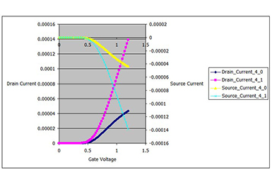
Gate Voltage Scanning Curve:
Vgs vs. Ids Curve:
When fixing Vds of a transistor, Ids varies when Vgs changes, forming a “Vgs vs. Ids” curve.
This curve can be used for studying how the carriers (electrons or “electric holes”) in the channel are raised to the conducting zone. Both the critical voltage at which a channel is formed and the critical voltage of a linear zone can be measured, providing important curves for the study of transistor characteristics.


 Weixin Service

 DouYin
 KuaiShou


