SERVICE

-
IC Counterfeit Detection
- IC Counterfeit Detection-Introduce
-
Non-Destructive Testing (NDT)
-
Destructive Testing
-
Value-Added Services
-
Destructive Physical Analysis (DPA)
- Destructive Physical Analysis (DPA)-Introduce
- External Visual Inspection
- X-Ray inspection
- Functional Testing (FT)
- Particle Impact Noise Detection (PIND/PIN-D)
- Hermeticity
- Internal Water Vapor
- Scanning Acoustic Tomography (SAT Testing)
- Solderability Test
- Decapsulation/Delid Test
- Bond Strength
- Die Shear Strength
- Configuration
-
Failure analysis
- Failure analysis-Introduce
-
Non-Destructive Analysis
-
Electrical Testing
-
Fault Location
-
Destructive Physical Analysis (DPA)
-
Physical Analysis
-
Engineering Sample (ES) Packaging Service
-
Competitor Analysis
-
Development and Functional Verification
- Development and Functional Verification-Introduce
-
New Product Development Testing (FT)
-
Key Functional Testing
-
Materials Analysis
- Materials Analysis-Introduce
-
FIB Circuit Edit
-
Structural Observation
-
Compositional Analysis
- EDS Analysis
-
Reliability Testing
- Reliability Testing-Introduce
-
Reliability Verification of Automotive Integrated Circuits (ICs)
-
Environmental Testing
-
Mechanical Testing
- Pull Test
- Die Strength Test
- High Strain Rate Test - Vibration Test
- Low Strain Rate Test - Bending Test
- High Strain Rate Test - Mechanical Shock Test
- Package Assembly Integrity Test - Wire Bonding Integrity
- Package Assembly Integrity Test
- Combined Vibration/Temperature/Humidity Test
- Combined Temperature/Humidity/Vibration/Altitude Test
- Free Fall Drop Test
- Box Compressive Strength Test
-
Corrosion Testing
-
IP Waterproof/Dust Resistant Test
-
Electromagnetic Compatibility (EMC)
- Electromagnetic Compatibility (EMC)-Introduce
- Immunity to Conducted Disturbances, Induced by Radio Frequency (RF) Fields
- Conducted Immunity Test
- Specific Absorption Rate (SAR) Testing for Electromagnetic Radiation
- Electrical Fast Transient/Burst (EFT/B) Test
- Voltage Flicker/Fluctuation Test
- Voltage Dips, Short Interruptions and Voltage Variations Immunity Test
- Power Frequency Magnetic Field (PFMF) Immunity Test
- Harmonic Interference Test
- Electrostatic Discharge (ESD) Immunity Test
- Surge/Lightning Immunity Test
- Radiated Emissions (RE) Test
- Radio Frequency (RF) Test
-
Chemical Analysis
- Chemical Analysis-Introduce
-
High-Performance Liquid Chromatography (HPLC)
-
Pyrolysis-Gas Chromatography-Mass Spectrometry (PY-GC-MS)
-
Inductively Coupled Plasma Optical Emission Spectroscopy (ICP-OES)
- Flame Retardancy Test
Description:
ESD (Electrostatic discharge) is the release of static electricity when two objects come into contact. Static electricity is a natural phenomenon with various generation methods such as contact or friction, etc. Static electricity is characterized by high voltage, low power, small current, and short duration.
EOS (Electrical Over-Stress) refers to all forms of excessive electrical stress. It is the thermal damage that may occur when an electronic device is subjected to a current or voltage that is beyond the specification limits of the device.
Latch-up refers to a condition where a low-impedance path in CMOS due to the interaction of parasitic PNP and NPN bipolar junction transistors between the power supply (VDD) and ground (GND or VSS) lines.
Latch-up is defined as the creation of a low impedance path between the power VDD and the ground VSS by the triggering of parasitic PNP and NPN bipolar structures (SCR’s) inherent in CMOS input and output circuitry.
Testing helps identify the vulnerabilities and electrostatic tolerance of ICs, providing a basis for subsequent system design adjustments, chip circuit design adjustments, and even RMA failure analysis.
Scope of Application:
Chip components and finished modules.
Test Modes:
Human Body Mode Test;
Machine Mode Test;
Charged Device Mode Test;
Latch-up Test;
Transient-Induced Latch up Test;
System ESD Test–ESD Gun Test;
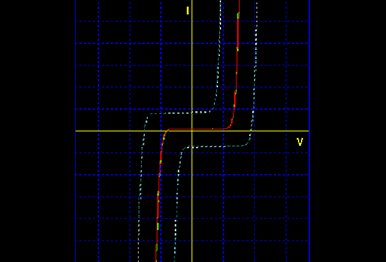
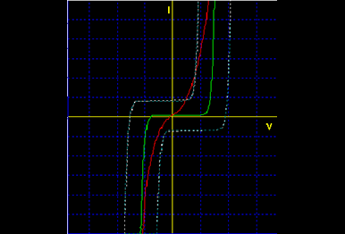
ESD I-V Curve Measurement;
Electrical Over Stress Test.
Gate Voltage Scanning Curve:
Voltage shift over ±30% at reference point.


Images of Testing Equipment:


 Weixin Service

 DouYin
 KuaiShou


