SERVICE

-
IC Counterfeit Detection
- IC Counterfeit Detection-Introduce
-
Non-Destructive Testing (NDT)
-
Destructive Testing
-
Value-Added Services
-
Destructive Physical Analysis (DPA)
- Destructive Physical Analysis (DPA)-Introduce
- External Visual Inspection
- X-Ray inspection
- Functional Testing (FT)
- Particle Impact Noise Detection (PIND/PIN-D)
- Hermeticity
- Internal Water Vapor
- Scanning Acoustic Tomography (SAT Testing)
- Solderability Test
- Decapsulation/Delid Test
- Bond Strength
- Die Shear Strength
- Configuration
-
Failure analysis
- Failure analysis-Introduce
-
Non-Destructive Analysis
-
Electrical Testing
-
Fault Location
-
Destructive Physical Analysis (DPA)
-
Physical Analysis
-
Engineering Sample (ES) Packaging Service
-
Competitor Analysis
-
Development and Functional Verification
- Development and Functional Verification-Introduce
-
New Product Development Testing (FT)
-
Key Functional Testing
-
Materials Analysis
- Materials Analysis-Introduce
-
FIB Circuit Edit
-
Structural Observation
-
Compositional Analysis
- EDS Analysis
-
Reliability Testing
- Reliability Testing-Introduce
-
Reliability Verification of Automotive Integrated Circuits (ICs)
-
Environmental Testing
-
Mechanical Testing
- Pull Test
- Die Strength Test
- High Strain Rate Test - Vibration Test
- Low Strain Rate Test - Bending Test
- High Strain Rate Test - Mechanical Shock Test
- Package Assembly Integrity Test - Wire Bonding Integrity
- Package Assembly Integrity Test
- Combined Vibration/Temperature/Humidity Test
- Combined Temperature/Humidity/Vibration/Altitude Test
- Free Fall Drop Test
- Box Compressive Strength Test
-
Corrosion Testing
-
IP Waterproof/Dust Resistant Test
-
Electromagnetic Compatibility (EMC)
- Electromagnetic Compatibility (EMC)-Introduce
- Immunity to Conducted Disturbances, Induced by Radio Frequency (RF) Fields
- Conducted Immunity Test
- Specific Absorption Rate (SAR) Testing for Electromagnetic Radiation
- Electrical Fast Transient/Burst (EFT/B) Test
- Voltage Flicker/Fluctuation Test
- Voltage Dips, Short Interruptions and Voltage Variations Immunity Test
- Power Frequency Magnetic Field (PFMF) Immunity Test
- Harmonic Interference Test
- Electrostatic Discharge (ESD) Immunity Test
- Surge/Lightning Immunity Test
- Radiated Emissions (RE) Test
- Radio Frequency (RF) Test
-
Chemical Analysis
- Chemical Analysis-Introduce
-
High-Performance Liquid Chromatography (HPLC)
-
Pyrolysis-Gas Chromatography-Mass Spectrometry (PY-GC-MS)
-
Inductively Coupled Plasma Optical Emission Spectroscopy (ICP-OES)
- Flame Retardancy Test
Description:
Transmission Electron Microscope (TEM) is primarily an analysis technique in which a high-energy beam of electrons is transmitted through an ultra-thin specimen. It provides imaging with atomic-level resolution down to 0.1 nanometers, allowing the observation of material microstructures or lattice defects.
TEM can be used for analysis of material microstructure, lattice defect (dislocation), and chemical composition. With additional functions such as EDS (Energy Dispersive X-ray Spectroscopy), HAADF (High-Angle Annular Dark Field) Z-contrast imaging, and stress analysis, it can provide atomic-scale structural and compositional information, solving various processing challenges.
Scope of Application:
Microstructural analysis (lattice imaging);
Analysis of crystal defects and lattice defects (dislocation);
Elemental analysis (EA);
Electron diffraction pattern analysis;
Impurity and contamination source analysis.
Testing Images:
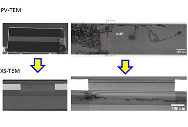
PV-TEM defect location to XS-TEM extended distribution analysis:
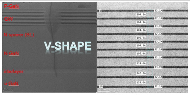
LED Epitaxial Structure Analysis: observation and measurement of LED epitaxial layer structure and LED quantum well.
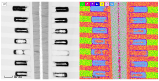
3D DRAM Analysis: analysis of 3D DRAM structure and 3D DRAM EDS mapping.
High-resolution TEM/EDS Analysis: 28nm HKMG transistor TEM image and 28nm HKMG transistor EDS mapping.
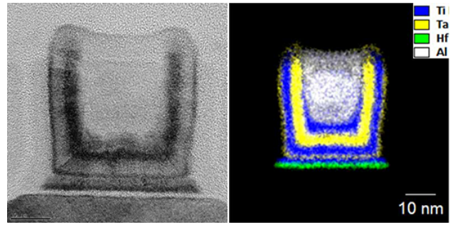
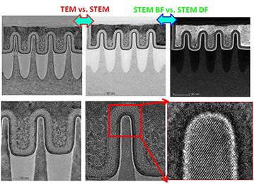
High-resolution TEM Image Analysis: advanced process FINFET images: high-magnification atomic images and STEM bright-field and dark-field images.
Images of Testing Equipment:
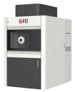
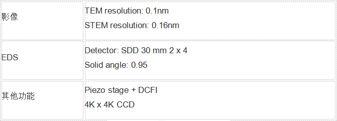
FEI Talos-F200X

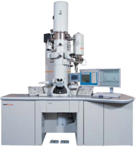
JEOL JEM-2100F
![]()


 Weixin Service

 DouYin
 KuaiShou


