SERVICE

-
IC Counterfeit Detection
- IC Counterfeit Detection-Introduce
-
Non-Destructive Testing (NDT)
-
Destructive Testing
-
Value-Added Services
-
Destructive Physical Analysis (DPA)
- Destructive Physical Analysis (DPA)-Introduce
- External Visual Inspection
- X-Ray inspection
- Functional Testing (FT)
- Particle Impact Noise Detection (PIND/PIN-D)
- Hermeticity
- Internal Water Vapor
- Scanning Acoustic Tomography (SAT Testing)
- Solderability Test
- Decapsulation/Delid Test
- Bond Strength
- Die Shear Strength
- Configuration
-
Failure analysis
- Failure analysis-Introduce
-
Non-Destructive Analysis
-
Electrical Testing
-
Fault Location
-
Destructive Physical Analysis (DPA)
-
Physical Analysis
-
Engineering Sample (ES) Packaging Service
-
Competitor Analysis
-
Development and Functional Verification
- Development and Functional Verification-Introduce
-
New Product Development Testing (FT)
-
Key Functional Testing
-
Materials Analysis
- Materials Analysis-Introduce
-
FIB Circuit Edit
-
Structural Observation
-
Compositional Analysis
- EDS Analysis
-
Reliability Testing
- Reliability Testing-Introduce
-
Reliability Verification of Automotive Integrated Circuits (ICs)
-
Environmental Testing
-
Mechanical Testing
- Pull Test
- Die Strength Test
- High Strain Rate Test - Vibration Test
- Low Strain Rate Test - Bending Test
- High Strain Rate Test - Mechanical Shock Test
- Package Assembly Integrity Test - Wire Bonding Integrity
- Package Assembly Integrity Test
- Combined Vibration/Temperature/Humidity Test
- Combined Temperature/Humidity/Vibration/Altitude Test
- Free Fall Drop Test
- Box Compressive Strength Test
-
Corrosion Testing
-
IP Waterproof/Dust Resistant Test
-
Electromagnetic Compatibility (EMC)
- Electromagnetic Compatibility (EMC)-Introduce
- Immunity to Conducted Disturbances, Induced by Radio Frequency (RF) Fields
- Conducted Immunity Test
- Specific Absorption Rate (SAR) Testing for Electromagnetic Radiation
- Electrical Fast Transient/Burst (EFT/B) Test
- Voltage Flicker/Fluctuation Test
- Voltage Dips, Short Interruptions and Voltage Variations Immunity Test
- Power Frequency Magnetic Field (PFMF) Immunity Test
- Harmonic Interference Test
- Electrostatic Discharge (ESD) Immunity Test
- Surge/Lightning Immunity Test
- Radiated Emissions (RE) Test
- Radio Frequency (RF) Test
-
Chemical Analysis
- Chemical Analysis-Introduce
-
High-Performance Liquid Chromatography (HPLC)
-
Pyrolysis-Gas Chromatography-Mass Spectrometry (PY-GC-MS)
-
Inductively Coupled Plasma Optical Emission Spectroscopy (ICP-OES)
- Flame Retardancy Test
Description:
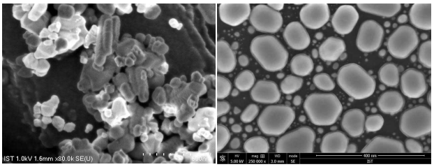
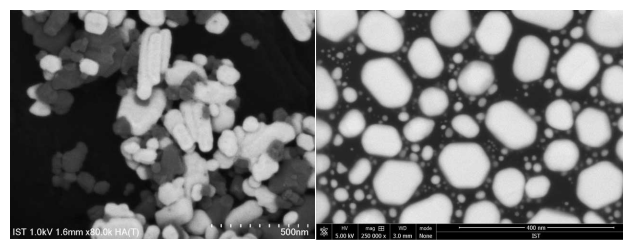
The Scanning Electron Microscope (SEM) uses optoelectronic system to focus electrons generated by an electronic gun onto a small spot on the sample surface. This beam of electrons will then interact with the sample material to generate secondary electrons, backscattered electrons, absorbed electrons, signature X-Ray and Auger electrons, etc. SEM collects the secondary electrons emitted from the surface of the sample to form an image of the sample surface.
Scope of Application:
Observation of surface microstructures of various materials;
SEM provides precise dimensional measurement;
EDS can be used for qualitative and semi-quantitative analysis of elemental composition on the sample surface, as well as point, line scan, or mapping analysis of specific areas;
EDS can even improve the mapping of spatial resolution under low voltage;
SEM automatic imaging with layer removal technique (de-process) can provide references for reverse engineering of electrical circuits;
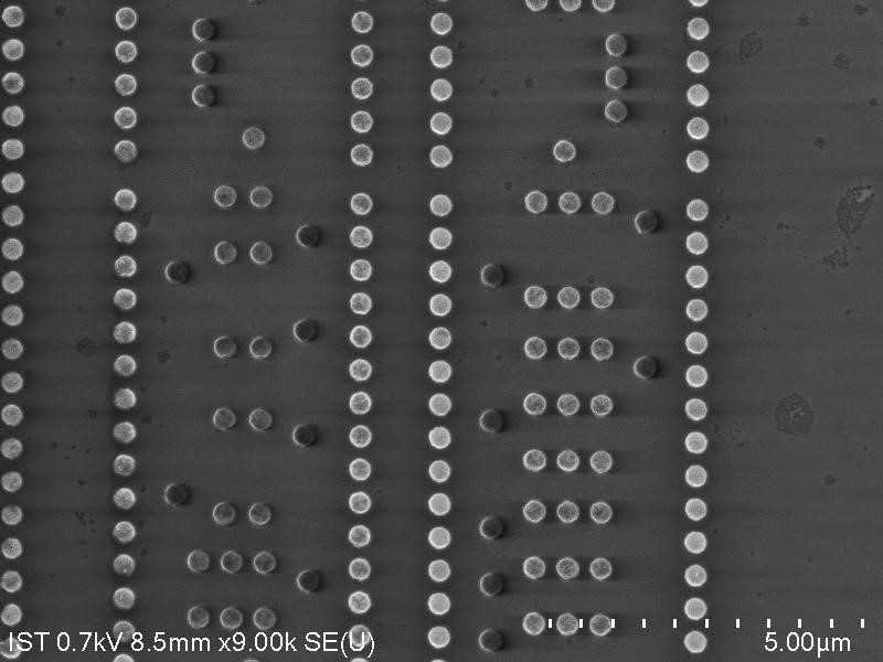
Passive Voltage Contrast (PVC) using low-energy electron beam scanning can accurately locate the electrical leakage or poor contact.
Features:
High resolution. The resolution of secondary electron imaging can reach 1nm (field emission) or 3nm (tungsten filament).
Large range of magnification adjustment (ranging from a few times to hundreds of thousands of times) and be continuously adjustable.
Large depth of field and sterescopic image, suitable for directly observing rough surfaces with significant surface undulations (such as fractured metals and ceramics).
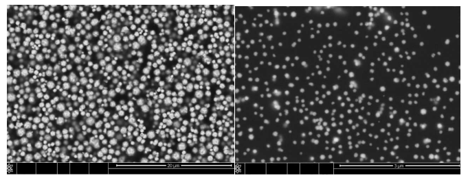
Surface Microstructure of Materials: Secondary Electrons Images
Surface Microstructure of Materials: Backscattered Electron Images
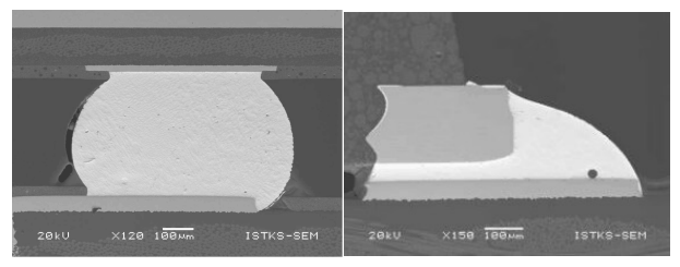
IC Cross-section View:
Passive Voltage Contrast (PVC): The contact open or short circuit can be diagnosed by the difference of brightness in the image.
Liquid Material Observation:
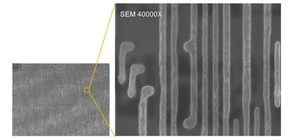
IC Reverse Engineering: By a SEM, the images of chip are captured over a large area; the left figure is mosaicked with 100 SEM images; the right figure is an enlarged part from the left which provides a clear visualization of the nano-grade circuit image.
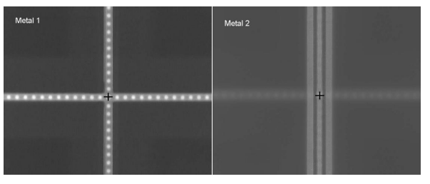
With stacked delayer and SEM image stitching, customers may view the the correspondence between different metal layers.
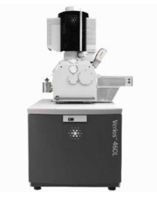
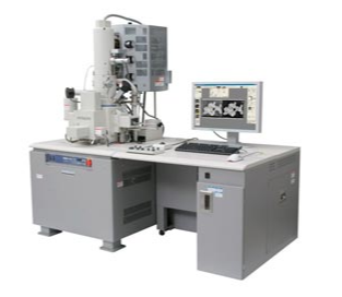
Images of Testing Equipment:
Thermo Fisher Verios 460L
HITACHI SU8220


 Weixin Service

 DouYin
 KuaiShou


