SERVICE

-
IC Counterfeit Detection
- IC Counterfeit Detection-Introduce
-
Non-Destructive Testing (NDT)
-
Destructive Testing
-
Value-Added Services
-
Destructive Physical Analysis (DPA)
- Destructive Physical Analysis (DPA)-Introduce
- External Visual Inspection
- X-Ray inspection
- Functional Testing (FT)
- Particle Impact Noise Detection (PIND/PIN-D)
- Hermeticity
- Internal Water Vapor
- Scanning Acoustic Tomography (SAT Testing)
- Solderability Test
- Decapsulation/Delid Test
- Bond Strength
- Die Shear Strength
- Configuration
-
Failure analysis
- Failure analysis-Introduce
-
Non-Destructive Analysis
-
Electrical Testing
-
Fault Location
-
Destructive Physical Analysis (DPA)
-
Physical Analysis
-
Engineering Sample (ES) Packaging Service
-
Competitor Analysis
-
Development and Functional Verification
- Development and Functional Verification-Introduce
-
New Product Development Testing (FT)
-
Key Functional Testing
-
Materials Analysis
- Materials Analysis-Introduce
-
FIB Circuit Edit
-
Structural Observation
-
Compositional Analysis
- EDS Analysis
-
Reliability Testing
- Reliability Testing-Introduce
-
Reliability Verification of Automotive Integrated Circuits (ICs)
-
Environmental Testing
-
Mechanical Testing
- Pull Test
- Die Strength Test
- High Strain Rate Test - Vibration Test
- Low Strain Rate Test - Bending Test
- High Strain Rate Test - Mechanical Shock Test
- Package Assembly Integrity Test - Wire Bonding Integrity
- Package Assembly Integrity Test
- Combined Vibration/Temperature/Humidity Test
- Combined Temperature/Humidity/Vibration/Altitude Test
- Free Fall Drop Test
- Box Compressive Strength Test
-
Corrosion Testing
-
IP Waterproof/Dust Resistant Test
-
Electromagnetic Compatibility (EMC)
- Electromagnetic Compatibility (EMC)-Introduce
- Immunity to Conducted Disturbances, Induced by Radio Frequency (RF) Fields
- Conducted Immunity Test
- Specific Absorption Rate (SAR) Testing for Electromagnetic Radiation
- Electrical Fast Transient/Burst (EFT/B) Test
- Voltage Flicker/Fluctuation Test
- Voltage Dips, Short Interruptions and Voltage Variations Immunity Test
- Power Frequency Magnetic Field (PFMF) Immunity Test
- Harmonic Interference Test
- Electrostatic Discharge (ESD) Immunity Test
- Surge/Lightning Immunity Test
- Radiated Emissions (RE) Test
- Radio Frequency (RF) Test
-
Chemical Analysis
- Chemical Analysis-Introduce
-
High-Performance Liquid Chromatography (HPLC)
-
Pyrolysis-Gas Chromatography-Mass Spectrometry (PY-GC-MS)
-
Inductively Coupled Plasma Optical Emission Spectroscopy (ICP-OES)
- Flame Retardancy Test
Description:
Mechanical shock test is performed in the laboratory to simulate a series of impacts that a product may experience in its working environment to evaluate its functionality and identify potential performance failures. In the actual storage, transportation, and daily use, various impact environments are encountered, such as braking during vehicle running or collision during goods handling.
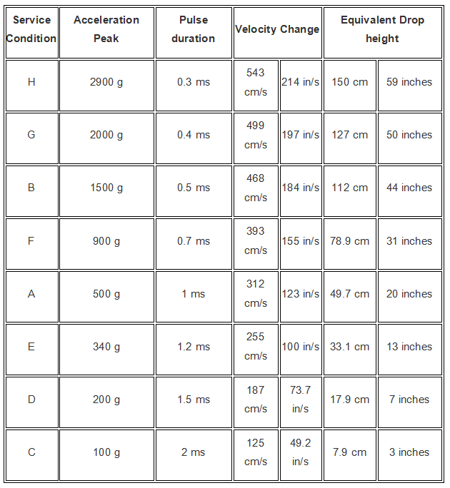
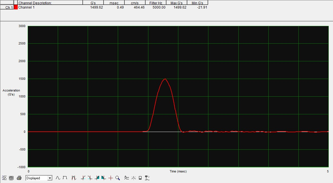
The technical parameters for the test include: peak acceleration, pulse duration, velocity change (half-sine wave, post-peak sawtooth wave, trapezoidal wave), and waveform selection. Conventional mechanical shock testing requires three impacts on each face, totaling 18 impacts on all six faces. Mechanical shock and impact testing can identify weak areas in the mechanical structure and evaluate the integrity and reliability of the product’s structure.
Mechanical shock usually produces high acceleration and short duration, resembling mechanical collisions in natural environments. Mechanical shock can have harmful effects on the structure and functional integrity of the product. Laboratory mechanical shock testing typically involves three types of waveforms: half-sine wave, trapezoidal wave (square wave), and triangular wave (leading and trailing sawtooth waves).
Purpose: The mechanical shock test is aimed to evaluate the ability of solder joints to withstand external stress caused by dynamic and severe bending during the manufacturing process, packing, shipping, and daily use of board-level IC packages and assess the impact on their lifespan.
Failure Mode: The mechanical shock test is aimed at verifying shock resistance of product and solder joints’ resistance against external stress at the moment of shock (high G-values). Real-time monitoring systems can be used to observe the product’s status during the test. Dye and pry or cross-section analysis can be performed afterward to observe the areas and extent of solder joint cracking.
Scope of Application:
ICs, components and other electrical and electronic products.
Testing Images:


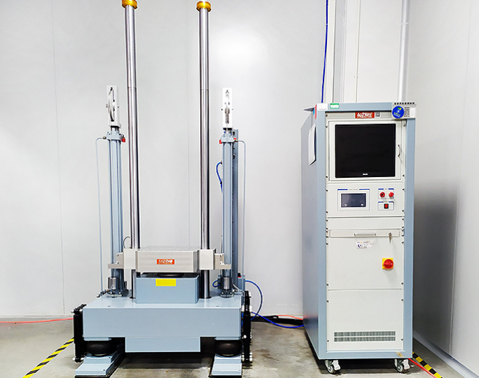
Image of Testing Equipment:


 Weixin Service

 DouYin
 KuaiShou


