SERVICE

-
IC Counterfeit Detection
- IC Counterfeit Detection-Introduce
-
Non-Destructive Testing (NDT)
-
Destructive Testing
-
Value-Added Services
-
Destructive Physical Analysis (DPA)
- Destructive Physical Analysis (DPA)-Introduce
- External Visual Inspection
- X-Ray inspection
- Functional Testing (FT)
- Particle Impact Noise Detection (PIND/PIN-D)
- Hermeticity
- Internal Water Vapor
- Scanning Acoustic Tomography (SAT Testing)
- Solderability Test
- Decapsulation/Delid Test
- Bond Strength
- Die Shear Strength
- Configuration
-
Failure analysis
- Failure analysis-Introduce
-
Non-Destructive Analysis
-
Electrical Testing
-
Fault Location
-
Destructive Physical Analysis (DPA)
-
Physical Analysis
-
Engineering Sample (ES) Packaging Service
-
Competitor Analysis
-
Development and Functional Verification
- Development and Functional Verification-Introduce
-
New Product Development Testing (FT)
-
Key Functional Testing
-
Materials Analysis
- Materials Analysis-Introduce
-
FIB Circuit Edit
-
Structural Observation
-
Compositional Analysis
- EDS Analysis
-
Reliability Testing
- Reliability Testing-Introduce
-
Reliability Verification of Automotive Integrated Circuits (ICs)
-
Environmental Testing
-
Mechanical Testing
- Pull Test
- Die Strength Test
- High Strain Rate Test - Vibration Test
- Low Strain Rate Test - Bending Test
- High Strain Rate Test - Mechanical Shock Test
- Package Assembly Integrity Test - Wire Bonding Integrity
- Package Assembly Integrity Test
- Combined Vibration/Temperature/Humidity Test
- Combined Temperature/Humidity/Vibration/Altitude Test
- Free Fall Drop Test
- Box Compressive Strength Test
-
Corrosion Testing
-
IP Waterproof/Dust Resistant Test
-
Electromagnetic Compatibility (EMC)
- Electromagnetic Compatibility (EMC)-Introduce
- Immunity to Conducted Disturbances, Induced by Radio Frequency (RF) Fields
- Conducted Immunity Test
- Specific Absorption Rate (SAR) Testing for Electromagnetic Radiation
- Electrical Fast Transient/Burst (EFT/B) Test
- Voltage Flicker/Fluctuation Test
- Voltage Dips, Short Interruptions and Voltage Variations Immunity Test
- Power Frequency Magnetic Field (PFMF) Immunity Test
- Harmonic Interference Test
- Electrostatic Discharge (ESD) Immunity Test
- Surge/Lightning Immunity Test
- Radiated Emissions (RE) Test
- Radio Frequency (RF) Test
-
Chemical Analysis
- Chemical Analysis-Introduce
-
High-Performance Liquid Chromatography (HPLC)
-
Pyrolysis-Gas Chromatography-Mass Spectrometry (PY-GC-MS)
-
Inductively Coupled Plasma Optical Emission Spectroscopy (ICP-OES)
- Flame Retardancy Test
Description:
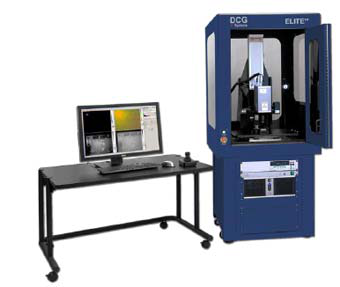
Thermal EMMI uses detector made of InSb to receive thermal radiation generated by a defective point after power-on, therefore positioning the defects (hot spots/bright spots); or, even estimating the depth of defects via time difference of thermal radiation transmission.
Scope of Application:
IC semiconductor industry, TFT LCD panel industry, PCB/PCBA industry.
Testing Content:
Detect the defect caused short-circuits inside IC packaging as well as sole die;
Current Leakage of dielectric layer (oxide);
Current Leakage in transistors and diodes;
Metal circuit defects and short-circuits in TFT LCD Panel & PCB/PCBA;
ESD latch-up;
Estimation the depth of the defect in 3D packaging (stacked die);
Defect positioning detection over non-decapped ICs;
Failure analysis over low impedance short circuit (<10ohm).
Testing Images:
IC Top Marking: IC Top Marking is clearly visible at low magnification.
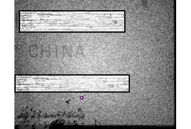
Low Impedance Short Circuit: In extremely low impedance of short-circuit samples, InGaAs and OBIRCH cannot detect bright spots, but thermal EMMI can successfully and clearly detect bright spots. The relative coordinates of the bright spots can be measured, which facilitates subsequent processes of delayering or cross-section positioning.
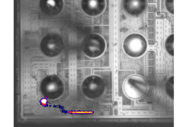
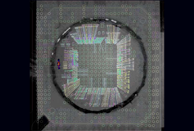
Detecting IC Without Decapsulation: IC defect can be clearly shown by hot spot imaging without de-capsulation of the IC. When combined with X-ray, it can clearly determine whether it is a bare die defect or a packaging issue.
Short Circuit in PCB: Short-circuit in PCB can also be revealed by hot spot imaging.
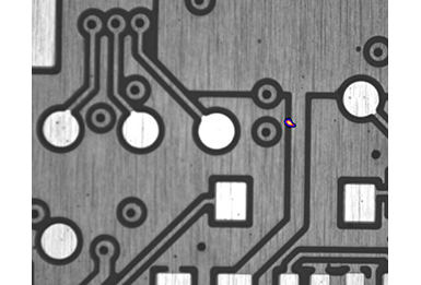
Image of Testing Equipment:


 Weixin Service

 DouYin
 KuaiShou


