SERVICE

-
IC Counterfeit Detection
- IC Counterfeit Detection-Introduce
-
Non-Destructive Testing (NDT)
-
Destructive Testing
-
Value-Added Services
-
Destructive Physical Analysis (DPA)
- Destructive Physical Analysis (DPA)-Introduce
- External Visual Inspection
- X-Ray inspection
- Functional Testing (FT)
- Particle Impact Noise Detection (PIND/PIN-D)
- Hermeticity
- Internal Water Vapor
- Scanning Acoustic Tomography (SAT Testing)
- Solderability Test
- Decapsulation/Delid Test
- Bond Strength
- Die Shear Strength
- Configuration
-
Failure analysis
- Failure analysis-Introduce
-
Non-Destructive Analysis
-
Electrical Testing
-
Fault Location
-
Destructive Physical Analysis (DPA)
-
Physical Analysis
-
Engineering Sample (ES) Packaging Service
-
Competitor Analysis
-
Development and Functional Verification
- Development and Functional Verification-Introduce
-
New Product Development Testing (FT)
-
Key Functional Testing
-
Materials Analysis
- Materials Analysis-Introduce
-
FIB Circuit Edit
-
Structural Observation
-
Compositional Analysis
- EDS Analysis
-
Reliability Testing
- Reliability Testing-Introduce
-
Reliability Verification of Automotive Integrated Circuits (ICs)
-
Environmental Testing
-
Mechanical Testing
- Pull Test
- Die Strength Test
- High Strain Rate Test - Vibration Test
- Low Strain Rate Test - Bending Test
- High Strain Rate Test - Mechanical Shock Test
- Package Assembly Integrity Test - Wire Bonding Integrity
- Package Assembly Integrity Test
- Combined Vibration/Temperature/Humidity Test
- Combined Temperature/Humidity/Vibration/Altitude Test
- Free Fall Drop Test
- Box Compressive Strength Test
-
Corrosion Testing
-
IP Waterproof/Dust Resistant Test
-
Electromagnetic Compatibility (EMC)
- Electromagnetic Compatibility (EMC)-Introduce
- Immunity to Conducted Disturbances, Induced by Radio Frequency (RF) Fields
- Conducted Immunity Test
- Specific Absorption Rate (SAR) Testing for Electromagnetic Radiation
- Electrical Fast Transient/Burst (EFT/B) Test
- Voltage Flicker/Fluctuation Test
- Voltage Dips, Short Interruptions and Voltage Variations Immunity Test
- Power Frequency Magnetic Field (PFMF) Immunity Test
- Harmonic Interference Test
- Electrostatic Discharge (ESD) Immunity Test
- Surge/Lightning Immunity Test
- Radiated Emissions (RE) Test
- Radio Frequency (RF) Test
-
Chemical Analysis
- Chemical Analysis-Introduce
-
High-Performance Liquid Chromatography (HPLC)
-
Pyrolysis-Gas Chromatography-Mass Spectrometry (PY-GC-MS)
-
Inductively Coupled Plasma Optical Emission Spectroscopy (ICP-OES)
- Flame Retardancy Test
Description:
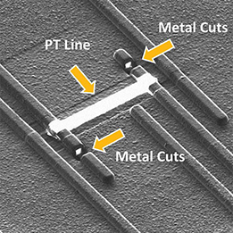
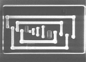
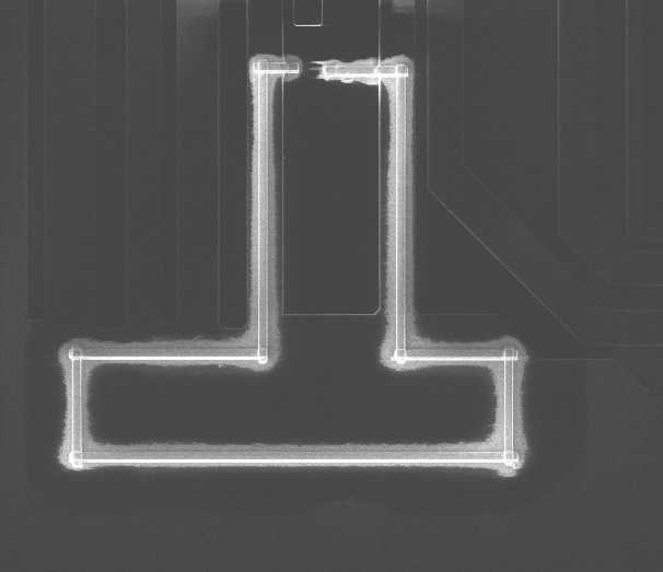
Focused Ion Beam (FIB) circuit edit is a technique that uses gallium ions to impact the surface of the sample and selectively etches (cuts) or deposits conductive or non-conductive materials (creates new circuits) using organic gases.
FIB circuit edit allows chip designers to directly edit the chip circuit without the need for repeated mask changes and reduces costs. It also accelerates the verification of chip design prototypes and time to market for mass production.
CAD probe pad fault detection is used to create signal acquisition points on the chip. It utilizes a FIB technique to extract the desired measurement signals from the chip designer and bring them to the chip’s surface. These signals are then captured using a mechanical prober to obtain internal chip signals.
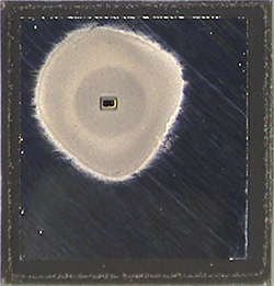
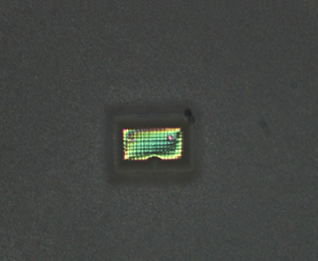
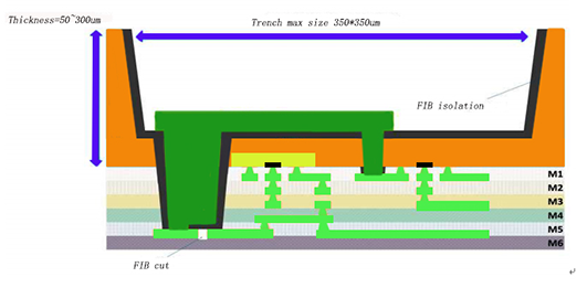
Wafer backside circuit edit: With the limitations of the package substrate in wafer-level packaging and the continuous advancement of advanced processes up to 7nm, accompanied by increased metal interconnect layers and more intricate and dense circuit layouts, the feasibility and success rate of circuit modification have been enhanced by performing modifications on the backside (Silicon) of the chip.
Scope of Application:
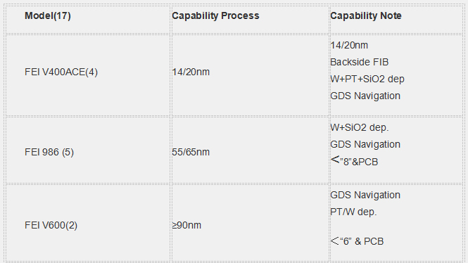
Up to 4.5nm resolution, capable of performing circuit edit in 16/14/10nm processes;
Maximum wafer size of 8 inches;
Available for Knights Merlin CAD Navigation software;
High-accuracy laser-guided Stage;
Built-in IR microscope for observing CMP layers and insulating silicon layers;
Two choices of metal deposition materials: tungsten (lower resistance) and platinum (faster speed);
Equipped with FEI DE/DX etching gas for high aspect ratio and dense circuits.
Testing Images:
Chip Front-Side Circuit Edit:
FIB CAD Probe Pad Fault Detection:

Complex Circuit Construction:
Adding Resistors inside the Chip Using FIB:
Wafer Backside Circuit Edit:
Testing Equipment Energy:
Suggestions to Improve Circuit Edit Yield:
Perform FIB after delayering, wire bonding, or packaging;
The more edits performed on the same chip, the higher the risk of failure;
FIB deposition has higher resistance compared to the original chip deposition. If there is a need for high current with low resistance, it should be specified beforehand;
Provide GDS II file for precise positioning (specific regions or layers) to enhance yield.


 Weixin Service

 DouYin
 KuaiShou


