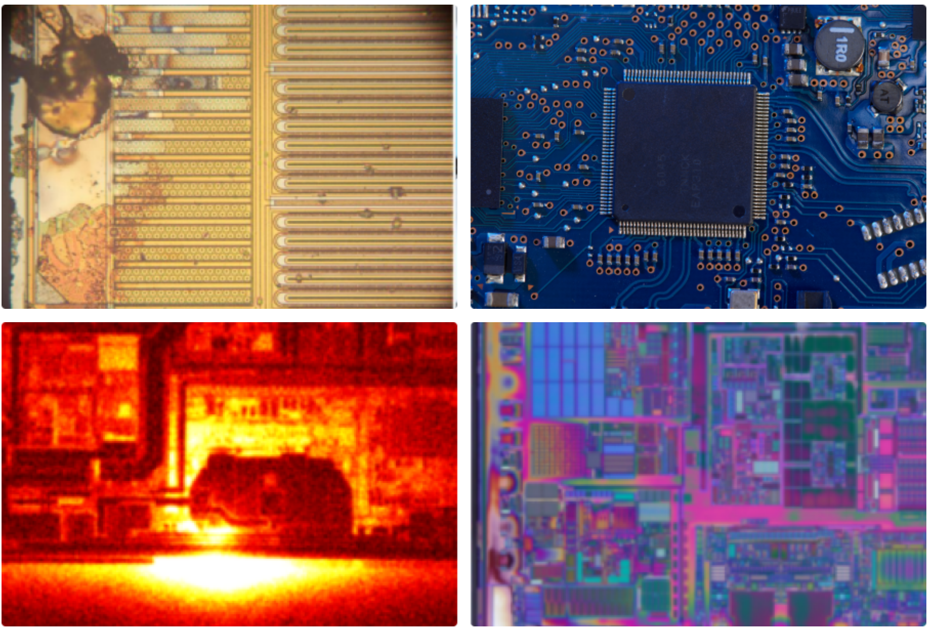
Through professional failure analysis equipment, various testing and analysis techniques, and analysis procedures, the failure phenomena of electronic components are identified, distinguishing their failure modes and failure mechanisms, determining the ultimate failure causes, and providing suggestions for improving design and manufacturing processes to prevent recurring failures.
Scope of Application:
Cause analysis of all failed components.
Basic Concepts of Failure Analysis:
1.Failure analysis often involves electrical measurements and the use of advanced physical, metallurgical, and chemical analysis methods.
2.The purpose of failure analysis is to determine failure modes and failure mechanisms, propose corrective measures, and prevent the repetition of these failure modes and mechanisms.
3.Failure mode refers to the observed failure phenomena or forms, such as open circuits, short circuits, parameter drift, functional failure, etc.
4.Failure mechanism refers to the physical and chemical processes leading to failure, such as fatigue, corrosion, overstress, etc.
Significance of Failure Analysis:
1. Failure analysis is a necessary means to determine the failure mechanisms of chips.
2. Failure analysis provides necessary information for effective fault diagnosis.
3. Failure analysis provides feedback information for design engineers to continuously improve or repair chip designs to align with design specifications.
4. Failure analysis can evaluate the effectiveness of different test vectors, provide necessary supplements for production testing, and offer essential information for optimizing verification test processes.
Main Steps and Contents of Failure Analysis:
IC Decapsulation:
Removal of IC encapsulation, while preserving the functionality of the chip without damage, including the die, bond pads, bond wires, and even the lead frame, to prepare for subsequent chip failure analysis experiments.
SEM/EDX Elemental Analysis:
Includes structural analysis/defect observation, routine micro-area analysis of element composition, accurate measurement of component dimensions, etc.
Probe Testing: Quickly and conveniently obtain internal electrical signals of ICs by means of probes.
Laser Cutting:
Using a micro laser beam to cut specific areas on the circuit or chip surface.
EMMI Detection:
EMMI is a highly efficient failure analysis tool that provides high-sensitivity non-destructive fault localization by detecting and locating very weak light emissions (visible and near-infrared) related to various component defects or abnormalities, such as leakage current visible light.
OBIRCH Application:
OBIRCH is commonly used for high-impedance and low-impedance analysis inside chips, as well as leakage path analysis in circuits. It can effectively locate defects in the circuit with OBIRCH method, such as voids in lines and under vias, high impedance areas at the bottom of vias, and can also detect short circuits or leakage. It is a powerful complement to photoluminescence technology.
LG Thermal Spot Detection:
Using liquid crystals to detect molecular rearrangements at leakage points in ICs, presenting as distinct spot-like patterns under a microscope, to identify leakage areas (fault points exceeding 10mA) that can trouble design personnel during practical analysis.
LG Thermal Spot Detection:
Using liquid crystals to detect molecular rearrangements at leakage points in ICs, presenting as distinct spot-like patterns under a microscope, to identify leakage areas (fault points exceeding 10mA) that can trouble design personnel during practical analysis.
X-ray Non-destructive Inspection:
Inspecting various defects in IC packaging, such as delamination, cracking, voids, and wire bond integrity, as well as possible defects in PCB processes, such as misalignment or bridging, open circuits, short circuits, or abnormal connections, and the integrity of solder balls in packaging.
SAM/SAT Ultrasonic Testing:
Non-destructive testing of internal structures in IC packages to effectively detect various damages caused by moisture or thermal energy, such as delamination of the die surface; cracks in solder balls, wafers, or encapsulation; internal voids in packaging materials; and various types of holes in die-bond surfaces, solder balls, encapsulation, etc.
Images of Failure analysis:


 Weixin Service

 DouYin
 KuaiShou


